ADT7463 查看數據表(PDF) - ON Semiconductor
零件编号
产品描述 (功能)
生产厂家
ADT7463 Datasheet PDF : 52 Pages
| |||
ADT7463
2. Data is sent over the serial bus in sequences of nine clock
pulses, eight bits of data followed by an Acknowledge Bit
from the slave device. Transitions on the data line must
occur during the low period of the clock signal and remain
stable during the high period, as a low-to-high transition
when the clock is high may be interpreted as a STOP signal.
The number of data bytes that can be transmitted over the
serial bus in a single READ or WRITE operation is limited
only by what the master and slave devices can handle.
3. When all data bytes have been read or written, stop conditions
are established. In WRITE mode, the master pulls the data line
high during the tenth clock pulse to assert a STOP condition.
In READ mode, the master device overrides the acknowledge
bit by pulling the data line high during the low period before
the ninth clock pulse. This is known as No Acknowledge.
The master then takes the data line low during the low pe-
riod before the 10th clock pulse, and then high during the
10th clock pulse to assert a STOP condition.
Any number of bytes of data can be transferred over the serial
bus in one operation, but it is not possible to mix read and write
in one operation because the type of operation is determined at
the beginning and cannot subsequently be changed without
starting a new operation.
In the case of the ADT7463, write operations contain either one
or two bytes, and read operations contain one byte and perform
the following functions.
To write data to one of the device data registers or read data from
it, the address pointer register must be set so that the correct data
register is addressed, then data can be written into that register
or read from it. The first byte of a write operation always contains
an address that is stored in the address pointer register. If data
is to be written to the device, then the write operation contains
a second data byte that is written to the register selected by the
address pointer register.
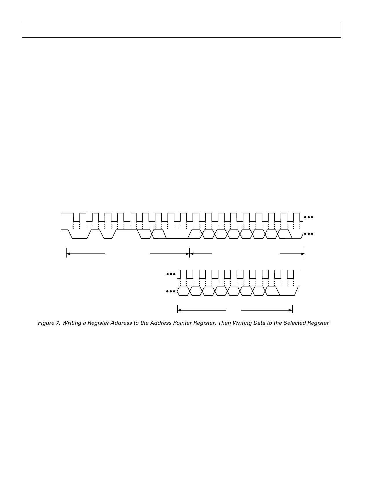
This is illustrated in Figure 7. The device address is sent over
the bus followed by R/W being set to 0. This is followed by two
data bytes. The first data byte is the address of the internal data
register to be written to, which is stored in the address pointer
register. The second data byte is the data to be written to the
internal data register.
1
9
1
9
SCL
SDA
0
1
START BY
MASTER
0
1
1 A1
FRAME 1
SERIAL BUS ADDRESS
BYTE
A0 R/W
D7
ACK. BY
ADT7463
1
SCL (CONTINUED)
D6 D5 D4 D3 D2 D1 D0
FRAME 2
ADDRESS POINTER REGISTER BYTE
ACK. BY
ADT7463
9
SDA (CONTINUED)
D7 D6 D5 D4 D3 D2 D1 D0
FRAME 3
DATA
BYTE
ACK. BY STOP BY
ADT7463 MASTER
Figure 7. Writing a Register Address to the Address Pointer Register, Then Writing Data to the Selected Register
Rev. 4 | Page 10 of 52 | www.onsemi.com
–10–
REV. C
Share Link: 