ADT7475 وں¥çœ‹و•¸و“ڑè،¨ï¼ˆPDF) - Analog Devices
零ن»¶ç¼–هڈ·
ن؛§ه“پوڈڈè؟° (هٹں能)
ç”ںن؛§هژ‚ه®¶
ADT7475 Datasheet PDF : 68 Pages
| |||
ADT7475
Parameter
DIGITAL INPUT LOGIC LEVELS (TACH INPUTS)
Input High Voltage, VIH
Min
Typ
Max
2.0
3.6
Unit Test Conditions/Comments
V
V
Maximum input voltage
Input Low Voltage, VIL
Hysteresis
0.8
−0.3
0.5
V
V
V p-p
Minimum input voltage
DIGITAL INPUT LOGIC LEVELS (THERM) ADTL+
Input High Voltage, VIH
Input Low Voltage, VIL
DIGITAL INPUT CURRENT
Input High Current, IIH
Input Low Current, IIL
Input Capacitance, CIN
SERIAL BUS TIMING2
Clock Frequency, fSCLK
Glitch Immunity, tSW
Bus Free Time, tBUF
SCL Low Time, tLOW
SCL High Time, tHIGH
SCL, SDA Rise Time, tr
SCL, SDA Fall Time, tf
Data Setup Time, tSU;DAT
Detect Clock Low Timeout, tTIMEOUT
0.75 أ— VCC V
0.4
V
آ±1
آ±1
5
10
4.7
4.7
4.0
250
15
400
50
50
1000
300
35
آµA
VIN = VCC
آµA
VIN = 0
pF
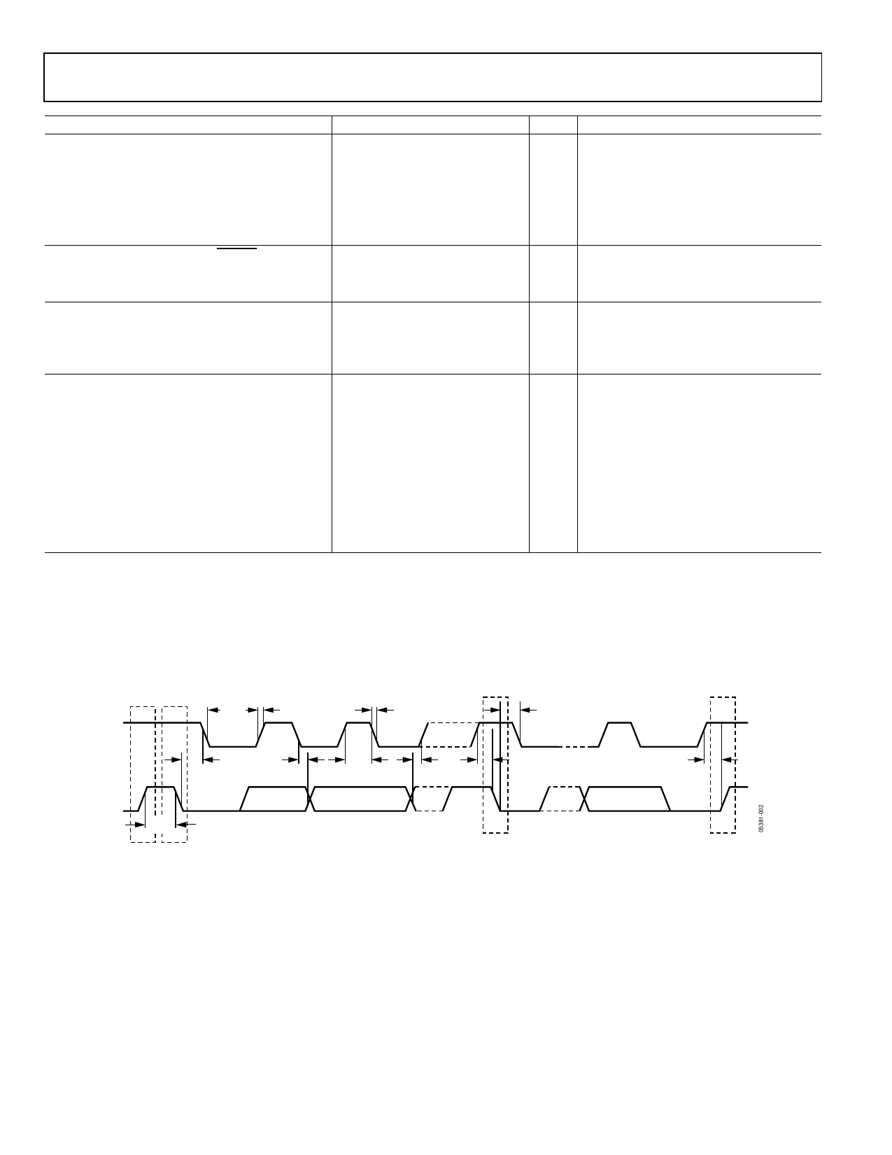
See Figure 2
kHz
ns
آµs
آµs
آµs
ns
آµs
ns
ms Can be optionally disabled
1 All voltages are measured with respect to GND, unless otherwise specified. Typicals are at TA = 25آ°C and represent most likely parametric norm. Logic inputs accept
input high voltages up to VMAX even when device is operating down to VMIN. Timing specifications are tested at logic levels of VIL = 0.8 V for a falling edge, and VIH =
2.0 V for a rising edge.
2 SMBus timing specifications are guaranteed by design and are not production tested.
TIMING DIAGRAM
SCL
tR
tLOW
tHD;STA
tHD;DAT
SDA
tBUF
P
S
tF
tHIGH
tSU;DAT
tHD;STA
tSU;STA
S
Figure 2. Serial Bus Timing Diagram
tSU;STO
P
Rev. A | Page 4 of 68
Share Link: 