AH212-EG 查看數據表(PDF) - WJ Communications => Triquint
零件编号
产品描述 (功能)
生产厂家
AH212-EG Datasheet PDF : 12 Pages
| |||
AH212
The Communications Edge TM
1 Watt High Linearity, High Gain InGaP HBT Amplifier
Product Information
Product Features
Product Description
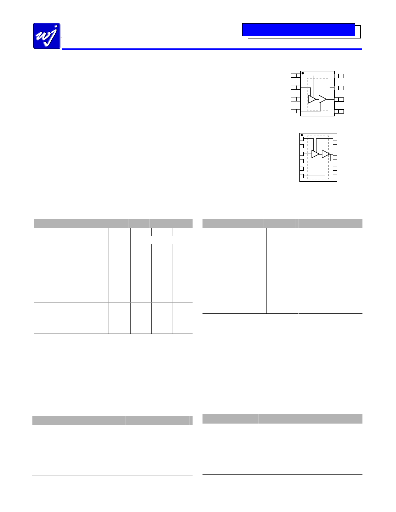
Functional Diagram
1800 – 2400 MHz
26 dB Gain
+30 dBm P1dB
+46 dBm Output IP3
+5V Single Positive Supply
Internal Active Bias
The AH212 is a high dynamic range two-stage driver
amplifier in a low-cost surface mount package. The
InGaP/GaAs HBT is able to achieve superior performance
for various narrowband-tuned application circuits with up
to +46 dBm OIP3 and +30 dBm of compressed 1-dB
power. The amplifier is available in an industry-standard
SMT lead-free/green/RoHS-compliant SOIC-8 or 4x5mm
DFN package. All devices are 100% RF and DC tested.
Lead-free/green/RoHS-compliant
SOIC-8 & 4x5mm DFN Package
Applications
Mobile Infrastructure
The product is targeted for use as linear driver amplifier for
various current and next generation wireless technologies
such as GPRS, GSM, CDMA, W-CDMA, TD-SCDMA,
and WiBro, where high linearity and high power is
required. The internal active bias allows the AH212 to
maintain high linearity over temperature and operate
directly off a +5 V supply.
WiBro Infrastructure
TD-SCDMA
Vcc1 1
8 N/C
Vbias1 2
RF In 3
7 Vcc2 / RF Out
6 Vcc2 / RF Out
Vbias2 4
5 N/C
AH212-S8G
Vbias1 1
N/C 2
RF In 3
N/C 4
N/C 5
Vbias2 6
12 Vcc1
11 N/C
10 Vcc2 / RF Out
9 Vcc2 / RF Out
8 N/C
7 N/C
AH212-EG
Specifications (1)
Parameters
Operational Bandwidth
Test Frequency
Gain
Input Return Loss
Output Return Loss
Output P1dB
Output IP3 (2)
Noise Figure
W-CDMA Channel Power
@ -45 dBc ACLR
Operating Current Range , Icc
Stage 1 Amp Current, Icc1
Stage 2 Amp Current, Icc2
Device Voltage, Vcc
Units
MHz
MHz
dB
dB
dB
dBm
dBm
dB
dBm
mA
mA
mA
V
Min
1800
22.2
+29
+43.5
340
Typ
2140
25
25
9
+29.5
+46
6.0
+21
400
85
315
5
Max
2400
500
1. Test conditions unless otherwise noted: 25 ºC, +5V, in tuned application circuit.
2. 3OIP measured with two tones at an output power of +15 dBm/tone separated by 1 MHz. The
suppression on the largest IM3 product is used to calculate the 3OIP using a 2:1 rule.
Typical Performance (1)
Parameters
Frequency
Gain (3)
Input Return Loss
Output Return Loss
Output P1dB (3)
Output IP3
IS-95A Channel Power
@ -45 dBc ACPR
W-CDMA Channel Power
@ -45 dBc ACLR
Noise Figure
Supply Bias
Units
MHz
dB
dB
dB
dBm
dBm
dBm
dBm
dB
Typical
1960
2140
25.8
25
15
25
11
9
+30
+29.5
+48.5
+46
+23.5
+21
5.5
6.0
+5 V @ 400 mA
3. The performance is shown for the AH212-S8G (SOIC-8 package) at 25ºC. The AH212-EG in a 4x5
mm DFN package offers approximately 0.5dB more gain and 0.5 dB higher P1dB.
Absolute Maximum Rating
Ordering Information
Parameter
Operating Case Temperature
Storage Temperature
RF Input Power (continuous)
Device Voltage
Device Current
Device Power
Junction Temperature
Rating
-40 to +85 C
-65 to +150 C
+26 dBm
+7 V
900 mA
5W
+250 ºC
Part No.
AH212-S8G
AH212-EG
AH212-S8PCB1960
AH212-S8PCB2140
AH212-EPCB1960
AH212-EPCB2140
Description
1 Watt, High Gain InGaP HBT Amplifier
(lead-free/green/RoHS-compliant SOIC-8 package)
1 Watt, High Gain InGaP HBT Amplifier
(lead-free/green/RoHS-compliant 12-pin 4x5mm DFN package)
1960 MHz Evaluation Board
2140 MHz Evaluation Board
1960 MHz Evaluation Board
2140 MHz Evaluation Board
Operation of this device above any of these parameters may cause permanent damage.
Specifications and information are subject to change without notice.
WJ Communications, Inc Phone 1-800-WJ1-4401 FAX: 408-577-6621 e-mail: sales@wj.com Web site: www.wj.com
Page 1 of 12 August 2006
Share Link: 