AIC1653CV 查看數據表(PDF) - Analog Intergrations
零件编号
产品描述 (功能)
生产厂家
AIC1653CV Datasheet PDF : 11 Pages
| |||
AIC1653
bursts by ramping up the inductor current, which is
then delivered to load. If either inductor value over
22µH or capacitor value under 4.7µF is used,
output ripple voltage will increase because the
capacitor will be slightly overcharged in each burst
cycle. Two methods of helping reduce output ripple
voltage are recommended. One is to increase the
output capacitor value. Adding a 100pF
feedforward capacitor that is parallel with R1 (see
Fig.13) is the other. And the addition of the small
capacitor will greatly reduce output ripple voltage.
Output Voltage Programming
A resistive divider, as in formula (3), sets the output
voltage.
( ) VOUT
=
−1.23V
1
+
R1
R2
+
R1×
2 × 10− 6
(3)
A capacitor at 100pF in parallel to the upper
feedback resistor is required for a stable feedback.
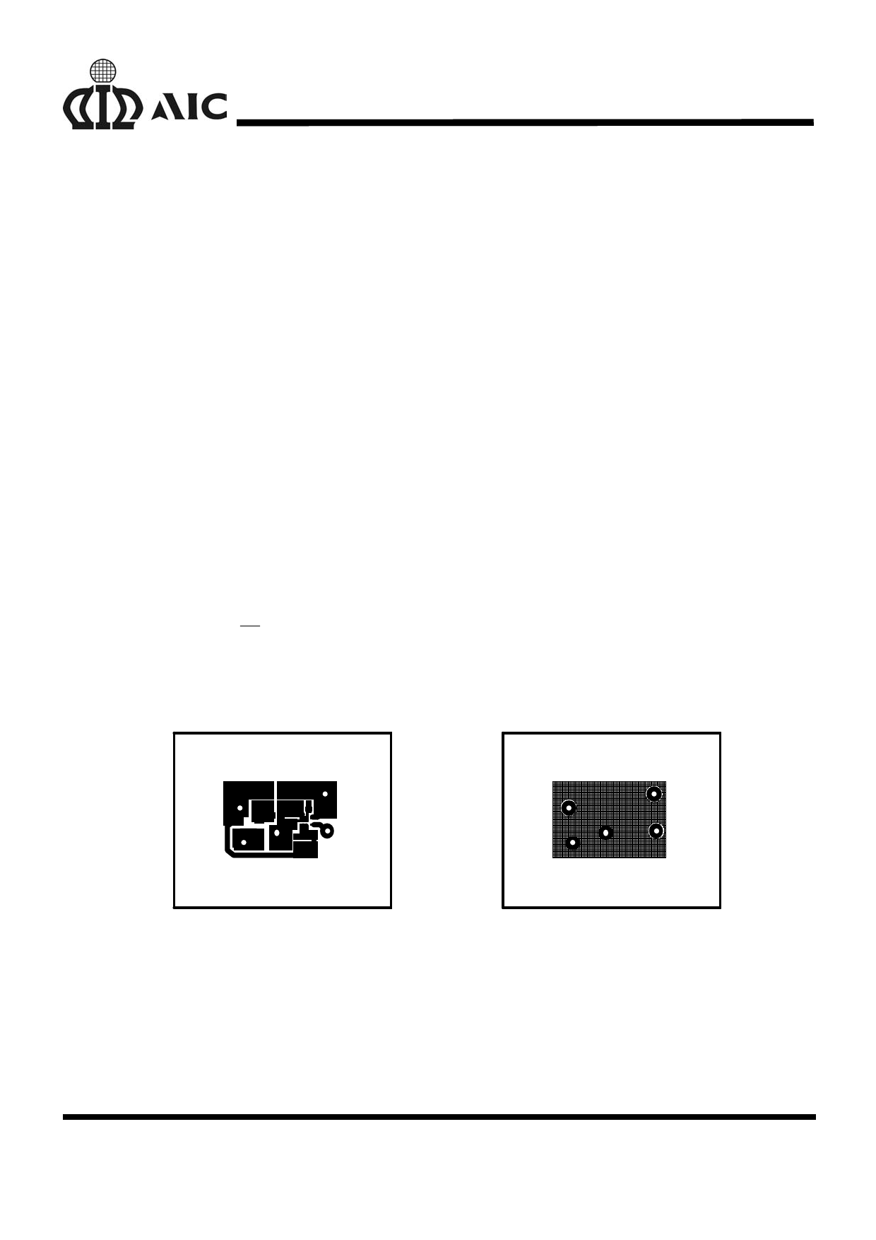
PCB Layout
Proper PCB layout and component placement may
enhance the performance of AIC1653 application
circuit. For a better efficiency, major loop from
input terminal to output terminal should be as short
as possible. In addition, in a case of a large current
loop, the track width of each component in the loop
should maintain as wide as possible. In order to get
rid of noise interference, separation of Schottky
diode ground and output terminal ground into two
independent parts is required. Recommended
layout diagrams and component placement are
shown as Fig. 9 to Fig. 12.
Fig. 9 Top Layer
Fig. 10 Bottom Layer
9
Share Link: 