M48Z35-70PC1TR жҹҘзңӢж•ёж“ҡиЎЁпјҲPDFпјү - STMicroelectronics
йӣ¶д»¶зј–еҸ·
дә§е“ҒжҸҸиҝ° (еҠҹиғҪ)
з”ҹдә§еҺӮ家
M48Z35-70PC1TR Datasheet PDF : 18 Pages
| |||
M48Z35, M48Z35Y
Table 4. AC Measurement Conditions
Input Rise and Fall Times
вүӨ 5ns
Input Pulse Voltages
0 to 3V
Input and Output Timing Ref. Voltages
1.5V
Note that Output Hi-Z is defined as the point where data is no longer
driven.
The SOIC and battery packages are shipped sep-
arately in plastic anti-static tubes or in Tape & Reel
form.
For the 28 lead SOIC, the battery package (i.e.
SNAPHAT) part number is "M4Z28-BR00SH1".
The M48Z35/35Y also has its own Power-fail De-
tect circuit. The control circuitry constantly moni-
tors the single 5V supply for an out of tolerance
condition. When VCC is out of tolerance, the circuit
write protects the SRAM, providing a high degree
of data security in the midst of unpredictable sys-
tem operation brought on by low VCC. As VCC falls
below approximately 3V, the control circuitry con-
nects the battery which maintains data until valid
power returns.
READ MODE
The M48Z35/35Y is in the Read Mode whenever
W (Write Enable) is high, E (Chip Enable) is low.
The device architecture allows ripple-through ac-
cess of data from eight of 264,144 locations in the
static storage array. Thus, the unique address
specified by the 15 Address Inputs defines which
one of the 32,768 bytes of data is to be accessed.
Valid data will be available at the Data I/O pins
within Address Access time (tAVQV) after the last
address input signal is stable, providing that the E
and G access times are also satisfied. If the E and
G access times are not met, valid data will be
available after the latter of the Chip Enable Access
time (tELQV) or Output Enable Access time
(tGLQV).
The state of the eight three-state Data I/O signals
is controlled by E and G. If the outputs are activat-
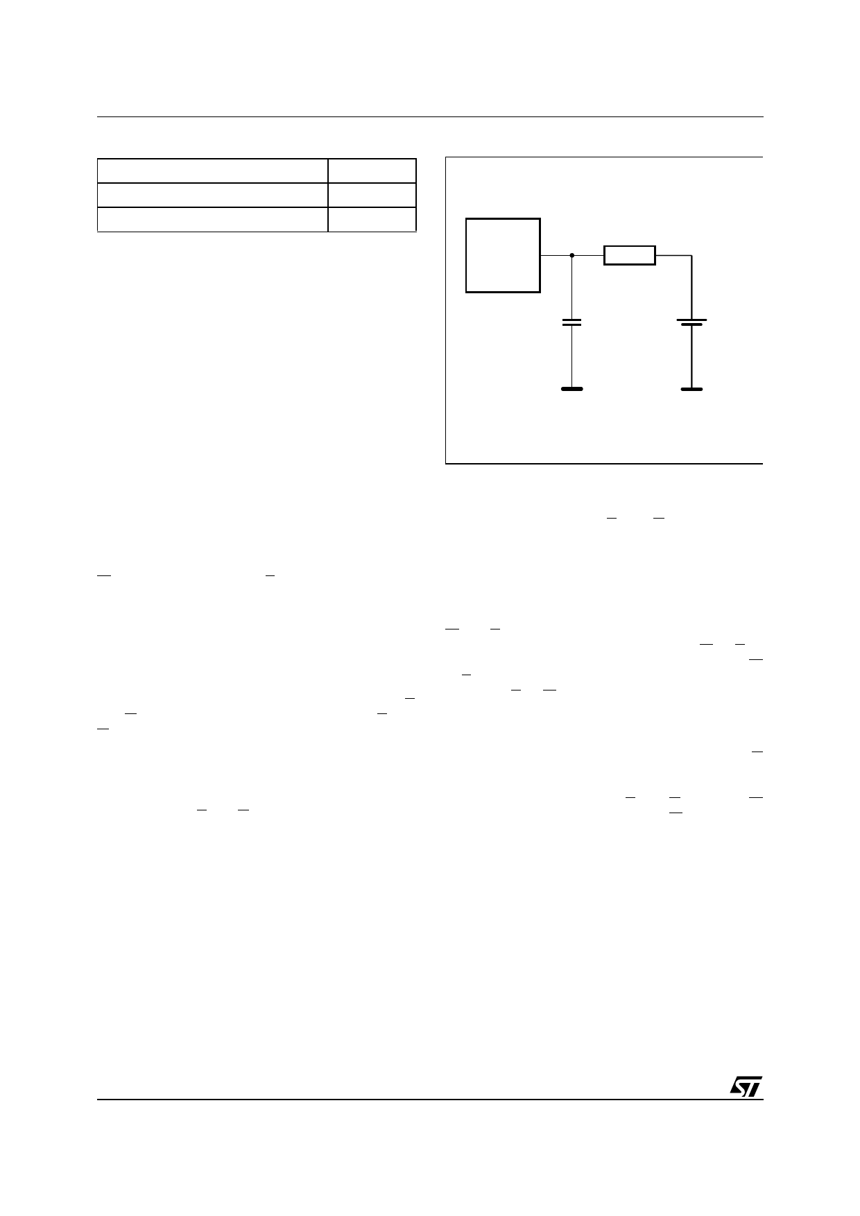
Figure 4. AC Testing Load Circuit
DEVICE
UNDER
TEST
645в„Ұ
CL = 100pF or
5pF
1.75V
CL includes JIG capacitance
AI03211
ed before tAVQV, the data lines will be driven to an
indeterminate state until tAVQV. If the Address In-
puts are changed while E and G remain active,
output data will remain valid for Output Data Hold
time (tAXQX) but will go indeterminate until the next
Address Access.
WRITE MODE
The M48Z35/35Y is in the Write Mode whenever
W and E are low. The start of a write is referenced
from the latter occurring falling edge of W or E. A
write is terminated by the earlier rising edge of W
or E. The addresses must be held valid throughout
the cycle. E or W must return high for a minimum
of tEHAX from Chip Enable or tWHAX from Write En-
able prior to the initiation of another read or write
cycle. Data-in must be valid tDVWH prior to the end
of write and remain valid for tWHDX afterward. G
should be kept high during write cycles to avoid
bus contention; although, if the output bus has
been activated by a low on E and G, a low on W
will disable the outputs tWLQZ after W falls.
4/18
Share Link: 