EDI8L32256C 查看數據表(PDF) - White Electronic Designs => Micro Semi
零件编号
产品描述 (功能)
生产厂家
EDI8L32256C Datasheet PDF : 5 Pages
| |||
Absolute Maximum Ratings*
Voltage on any pin relative to VSS
Operating Temperature TA (Ambient)
Commercial
Industrial
Storage Temperature
Power Dissipation
Output Current.
Junction Temperature, TJ
-0.5V to 7.0V
0°C to + 70°C
-40°C to +85°C
-55°C to +125°C
3.1 Watts
20 mA
175°C
*Stress greater than those listed under "Absolute Maximum Ratings" may cause
permanent damage to the device. This is a stress rating only and functional
operation of the device at these or any other conditions greater than those indicated
in the operational sections of this specification is not implied. Exposure to absolute
maximum rating conditions for extended periods may affect reliability.
Recommended DC Operating Conditions
Parameter
Sym Min Typ Max Units
Supply Voltage VCC 4.75 5.0 5.25 V
Supply Voltage VSS 0 0 0 V
Input High Voltage VIH 2.2 -- VCC+0.5 V
Input Low Voltage VIL -0.3 -- 0.8 V
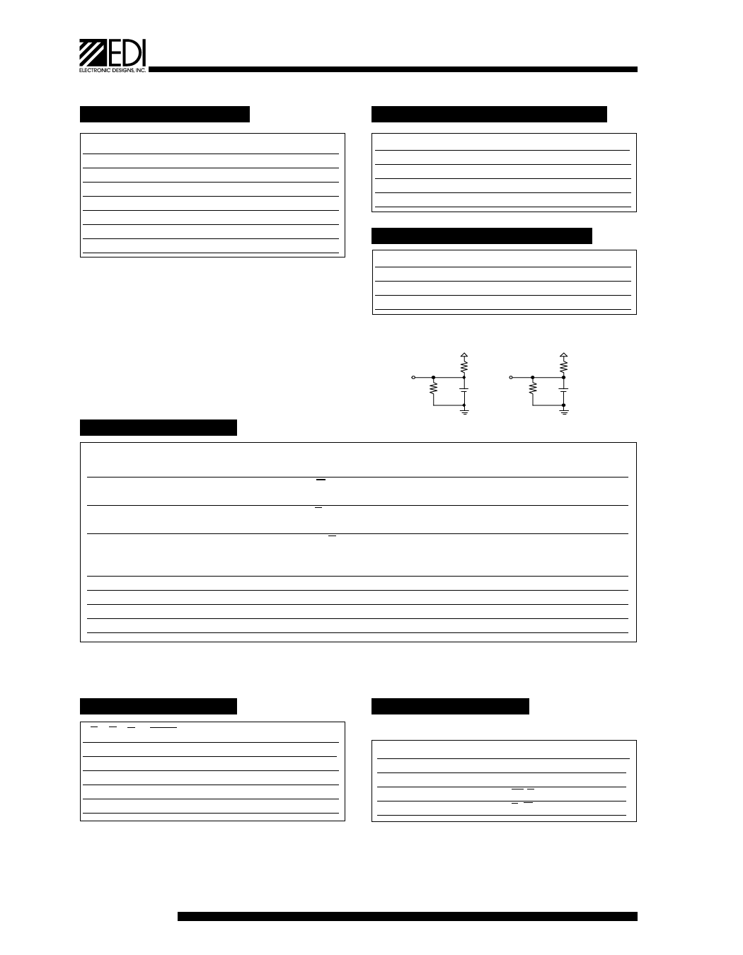
AC Test Conditions
Input Pulse Levels
Input Rise and Fall Times
Input and Output Timing Levels
Output Load
(note: For TEHQZ,TGHQZ and TWLQZ, CL = 5pF)
Figure 1
VCC
Figure 2
Q
255
480
30 pF
Q
255
VSS to 3.0V
5ns
1.5V
Figure 1
VCC
480
5 pF
DC Electrical Characteristics
Parameter
Sym
Operating Power Supply Current ICC1
Standby (TTL) Supply Current ICC2
Full StandbySupply Current
ICC3
Input Leakage Current
ILI
Output Leakage Current
ILO
Output High Volltage
VOH
Output Low Voltage
VOL
Conditions
Min
W= VIL, II/O = 0mA,
Min Cycle
E ≥ VIH, VIN ≤ VIL or
VIN ≥ VIH, f=ØMHz
E ≥ VCC-0.2V
VIN ≥ VCC-0.2V or
VIN ≤ 0.2V
VIN = 0V to VCC
V I/O = 0V to VCC
IOH = -4.0mA
2.4
IOL = 8.0mA
Max
15/17
575
120
20
Units
20/25
480 mA
120 mA
20 mA
±10
µA
±10
µA
V
0.4
V
Truth Table
E W G BSØ-3 Mode Output
H X X X Standby High Z
L H H X Output Disable High Z
L X X H Output Disable High Z
L H L L Read DOUT
L L X L Write
DIN
Power
ICC2,ICC3,
ICC1
ICC1
ICC1
ICC1
X Means Don't Care
Capacitance
(f=1.0MHz, VIN=VCC or VSS)
Parameter
Sym
Address Lines
CA
Data Lines
CD/Q
Write & Output Enable Lines W, G
Chip Enable Lines/Byte Select E, BS
Max Unit
20 pF
10 pF
6
pF
9
pF
EDI8L32256C
256Kx32 SRAM Module
2
EDI8L32256C Rev. 4 3/98 ECO#9662
Share Link: 