AN-9037 查看數據表(PDF) - Fairchild Semiconductor
零件编号
产品描述 (功能)
生产厂家
AN-9037 Datasheet PDF : 7 Pages
| |||
formula for calculating the area ratio for paste
release prediction:
Area Ratio =
Area of Pad
L *W
=
Area of Aperture Walls 2 * (L *W ) * T
Where L is the length, W the width, and T the
thickness of the stencil. When using this equation,
an Area Ratio >0.66 should yield acceptable paste
release. The recommended stencil apertures can
be found in the appendix.
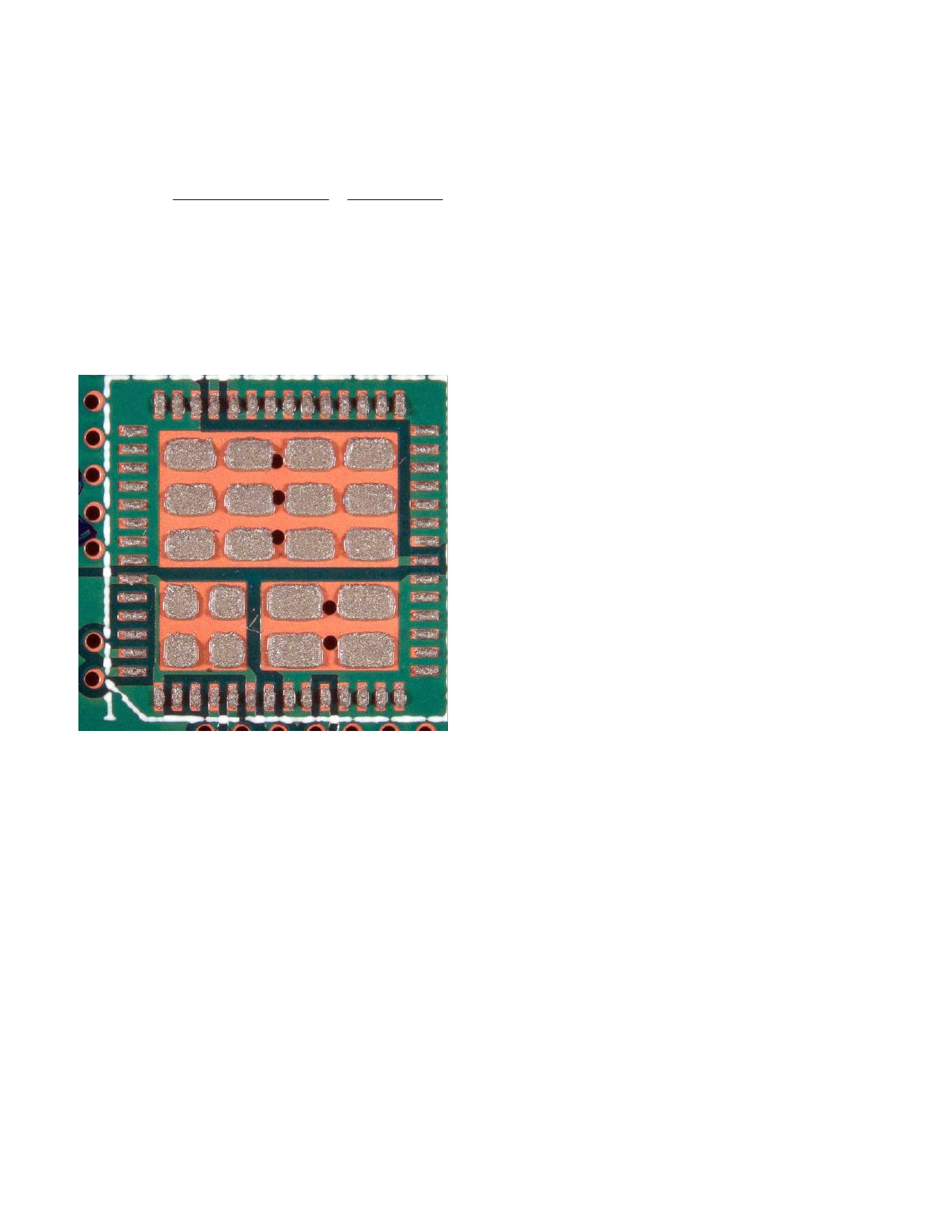
Figure 4: Printed Solder Paste.
SOLDER PASTE
The 8x8MLP is a RoHS compliant and lead free
package. The lead finish is NiPdAu. Any standard
lead free no clean solder paste commonly used in
the industry should work with this package. The
IPC Solder Products Value Council has
recommended that the lead free alloy, 96.5
Sn/3.0Au/0.5Cu, commonly known as SAC 305,
is “…the lead free solder paste alloy of choice for
the electronics industry”. Type 3 no-clean paste,
SAC 305 alloy, was used for the construction of
the boards studied to optimize the process.
REFLOW PROFILE
The optimum reflow profile used for every
product and oven is different. Even the same
brand and model oven in a different facility may
require a different profile. The proper ramp and
soak rates are determined by the solder paste
vendor for their products. Obtaining this
information from the paste vendor is highly
recommended. If one is using a KIC® profiler,
downloading the latest paste library from KIC®
will yield ramp rate and soak times at temperature
for most commonly used solder pastes. The
Fairchild 8x8 MLP is rated for 260ºC peak
temperature reflow. Below is a sample reflow
profile used for building demonstration boards.
Attached in the appendix is a reflow profile
example. This profile is provided for reference
only; different PWBs, ovens and pastes will change
this profile, perhaps dramatically.
VOIDING
Voiding is a very controversial topic in the
industry currently. The move to lead free solders,
due to various governmental regulations, has
created intense study in the area of solders, solder
joints and reliability effects. There are varying
viewpoints on the effect of vias and allowable
quantity. There are several types of voids
however; we will divide them into two classes,
macro-voids, and micro-voids.
Macro-voids could also be called process voids.
Macro voids are the large sized voids commonly
seen on x-ray during inspection. These voids are
due to process design/control issues, or PWB
design issues. All of the parameters discussed in
this application note will effect macro-voiding.
Most standards that currently exist, such as IPC-
610D specifically address void criteria for BGA,
and limit it to 25%. This standard is for macro-
voiding.
Fairchild has done several studies of the amount of
voiding in various types of components with large
thermal pads, and the effect on reliability. It was
found that components with 25% voiding or less
had acceptable reliability performance in package
Share Link: 