AN-9037 查看數據表(PDF) - Fairchild Semiconductor
零件编号
产品描述 (功能)
生产厂家
AN-9037 Datasheet PDF : 7 Pages
| |||
qualification temperature cycling. Fairchild gives
the customer the guideline of 25% voiding for
MLP type packages.
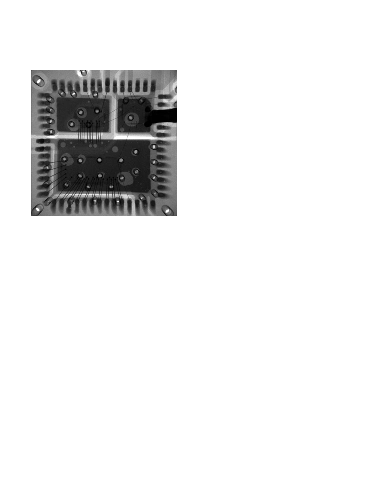
Figure 5: X-ray image showing voiding caused by
vias in pad.
There are also several forms of micro-voiding,
namely planar micro voids and Kirkendall voids.
The mechanism of void creation is different for
each; however both are practically undetectable by
x-ray inspection. Both types are also currently the
subject of several in-depth studies; however, none
have confirmed theories of creation.
Planar micro voids, or “champagne voids” occur
at the PWB land to solder joint interface. There
are several theories on the mechanism that creates
planar micro voids, but there is not a confirmed
root cause. Planar micro voids are a risk for
reliability failures.
Kirkendall voids are created at the interface of two
dissimilar metals at higher temperatures. In the
case of solder attachments, at the pad to joint
intermetallic layer. They are not due to the reflow
process; Kirkendall voids are created by electro-
migration in assemblies that spend large amounts
of time above 100ºC. There is currently
conflicting evidence whether Kirkendall voids are
a reliability risk or not.
REWORK
Due to the high temperatures associated with lead
free reflow, it is recommended that this
component not be reused if rework becomes
necessary. The MLP should be removed from the
PWB with hot air. After removal, the 8x8 MLP
should be discarded. The solder remnants should
be removed from the pad with a solder vacuum or
solder wick, the pads cleaned and new paste
printed with a mini stencil. Localized hot air can
then be applied to reflow the solder and make the
joint. Due to the thermal performance of this
component, and the typical high performance
PWB it will be mounted on, quite a bit of heat
energy will be necessary. Heating of the PWB may
be helpful for the rework process.
BOARD LEVEL RELIABILITY
As mentioned previously, per JDC-STD-001D a
solder fillet is not required on the side of the lead
for this package. But it has been found through
modeling and temperature cycling that a solder
fillet on the lead end can improve reliability. An
improvement of 20% can be expected with this
fillet. It was also found that if the fillet only wets
halfway up the side of the lead, this reliability
enhancement is still attained. Through process
control these fillets are often created.
As part of the standard reliability testing this
package was temperature cycled from -10 to 100C.
There could be no failures in the sample set at
1000 cycles to pass the test.
WORKS CITED
[1] Aspandiar, Raiyo, “Voids in Solder Joints,”
SMTA Northwest Chapter Meeting,
September 21, 2005, Intel Corporation
[2] Bryant, Keith, “Investigating Voids,”
Circuits Assembly, June 2004
[3] Comley, David, et al, “The QFN: Smaller,
Faster and Less Expensive,” Chip Scale
Review.com, August/September 2002
[4] Englemaier, Werner, “Voids in solder
joints-reoliability,” Global SMT & Package,
December 2005
Share Link: 