GTL2002 查看數據表(PDF) - Philips Electronics
零件编号
产品描述 (功能)
生产厂家
GTL2002 Datasheet PDF : 24 Pages
| |||
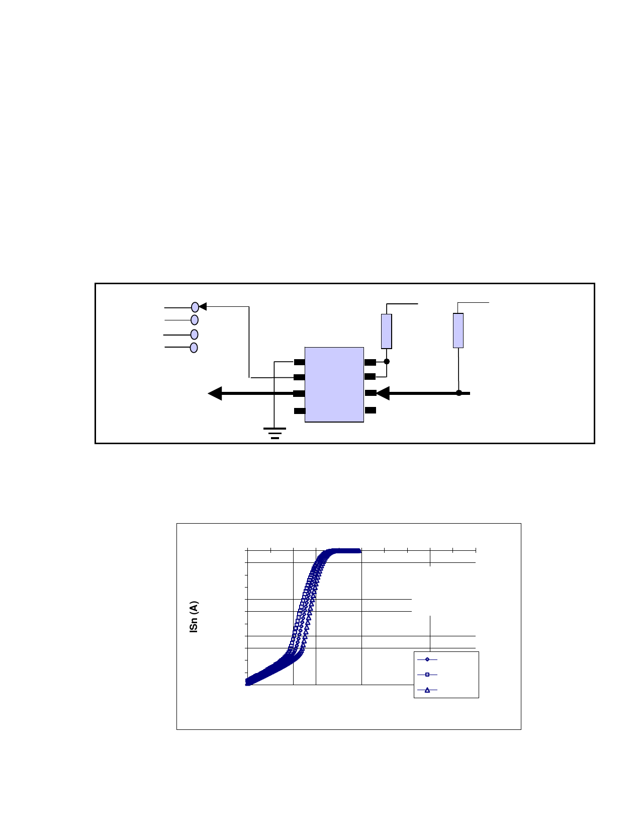
Figure 6 – GTL-TVC Typical Application Circuit
Propagation delay
Propagation delay for the GTL-TVC devices is problematic to define because, like the CBT functions, it is very small
across the transistor. The rise time is dominated by the RC time constant of the node, and the fall time is dominated by
the pull down driver, the total capacitance and the pull up resistor. The propagation delay is normally measured from ½
the swing on the lower voltage side to ½ the swing on the higher voltage side or vice versa. For a 0 V to 3 V transition on
the input with a 1 ns edge rate to a 0 V to 3 V output, the measurement points on both sides would be 1.5 V and the
propagation delay would be less than 1 ns. However, for a GTL+ to 5 V translation, where the pull up on the 5 V side is
2.2 k Ω and the total capacitance is 100 pF, the rising edge propagation would be measured from the 1 V point on the
GTL+ side to 2.5 V on the 5 V side and would measure about 95 ns because of the RC time constant.
GTL-TVC Electrical characteristics
The typical electrical characteristics of the GTL-TVC NMOS transistors as measured over temperature using the test
configuration shown in Figure 7 are included in Figures 8 to 13.
1.0 V
1.5 V
2.0 V
2.5 V
VSREF
VSn
VDDREF
GTL2002
GND GREF
SREF DREF
S1 D1
S2 D2
RDREF
VDDpass
RDn
VDn
Figure 7. GTL-TVC Test Set Up
0
0.00E+00
-2.00E-03
-4.00E-03
-6.00E-03
-8.00E-03
-1.00E-02
-1.20E-02
-1.40E-02
-1.60E-02
-1.80E-02
-2.00E-02
-2.20E-02
0.25 0.5 0.75
1 1.25 1.5 1.75 2 2.25 2.5
VDDref = 3.3v
VDDpass = 3.3v
RDn = 150 ohms
RDref = 200k
VSn (V)
Vsref = 1 V
25 deg C
85 deg C
-40 deg C
8
Share Link: 