AN7199Z 查看數據表(PDF) - Panasonic Corporation
零件编号
产品描述 (功能)
生产厂家
AN7199Z Datasheet PDF : 17 Pages
| |||
AN7199Z
ICs for Audio Common Use
s Technical Information (continued)
[2] Application note (continued)
2. Oscillation countermeasures
1
1) In order to increase the oscillation allowance, it is unnecessary to use a
capacitor and a resistor between each output terminal and GND. How-
ever, when inserting the capacitor for counter-measures against output
line noise between the output terminal and GND, insert a resistor of
approx. 2.2 Ω in series as shown in figure 2. The oscillation may occur
2,4
13,15
To speaker
0.01 µF to 0.1 µF
if only capacitor is used. Use it after giving a sufficient evaluation
2) The use of polyester film capacitor having a little fluctuation with tem-
perature and frequency is recommended as the capacitor for counter-
2.2 Ω
3,14
measures against output line noise.
3. Input terminal
Figure 2
1) The reference voltage of input terminal is 0 V. When the input signal has a reference voltage other than 0 V
potential, connect a coupling capacitor (of about several µF) for DC component cut in series with the input
terminal. Check the low-pass frequency characteristics to determine the capacitor value.
2) 10 kΩ or less of signal source impedance Rg can reduce the output end noise voltage.
3) The output offset voltage fluctuates when the signal source impedance Rg is changed. A care must be taken
when using the circuit by directly connecting the volume to the input terminal. In such a case, the use of
coupling capacitor is recommended.
4) If a high frequency signal from tuners enters the input terminal as noise, insert a capacitor of approx. 0.01 µF
between the input terminal and input GND.
When a high frequency signal is inputted, malfunction in protective circuits may occur.
15 µA 15 µA
1 µF
Input signal
0.01 µF
6 200 Ω
11
10 kΩ 30 kΩ
600 Ω
To power
Attenuator
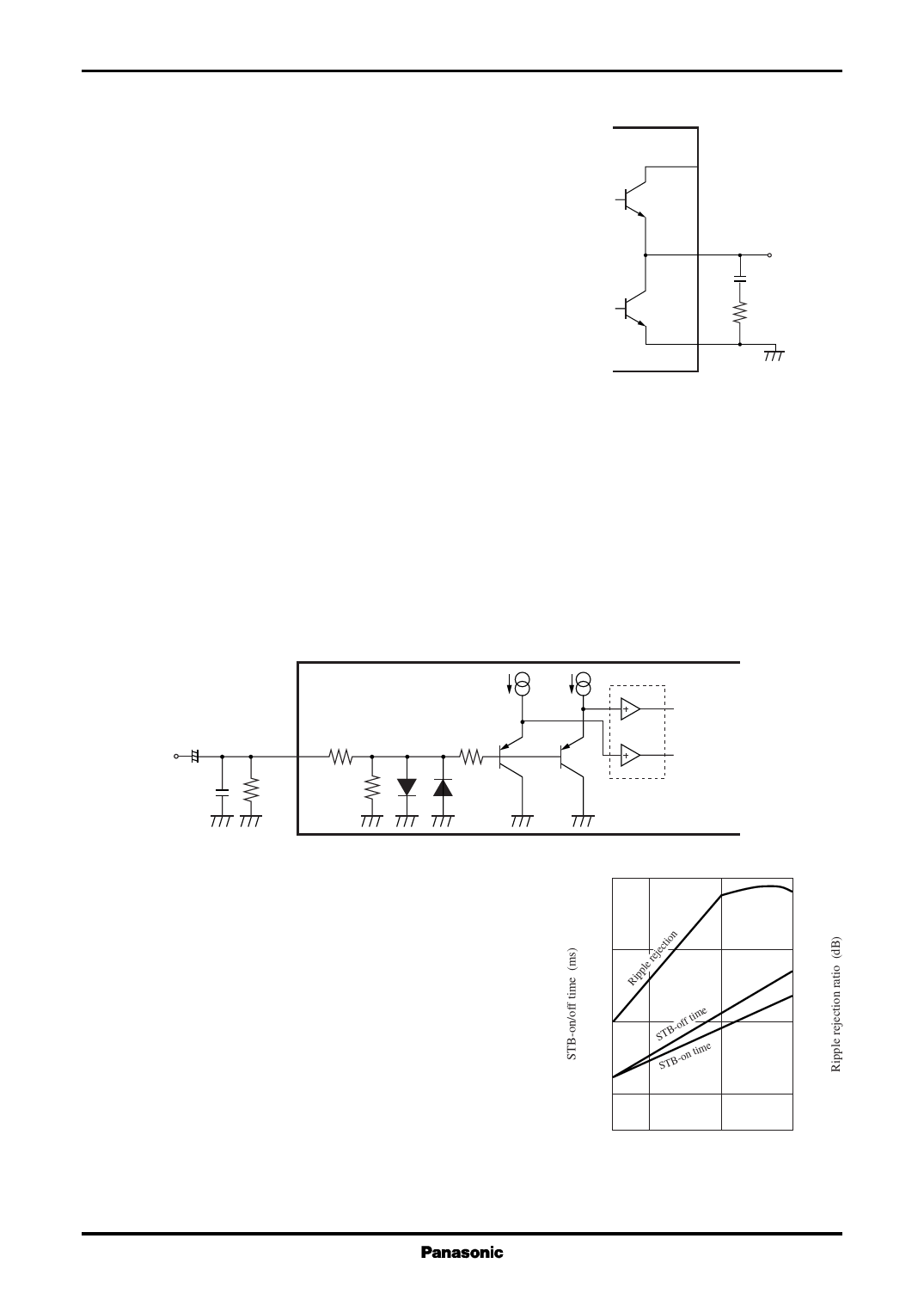
4. Ripple filter
Figure 3
1) In order to suppress the fluctuation of supply voltage, connect
a capacitor of approx. 33 µF between RF terminal (pin12) and
GND.
2) Relation between RR (Ripple Rejection Ratio) and a capacitor 1 000
The larger the capacitance of the ripple filter is, the better the
ripple rejection becomes.
100
3) Relation between the rise time of circuit and a capacitor
The larger the capacitance of the ripple filter is, the longer the
time from the power on (standby high) to the sound release
becomes.
10
4) The DC voltage of output terminal is approximately the middle
point of the ripple filter terminal voltage.
5) The internal circuit of ripple filter terminal is as shown in fig-
ure 5 and the charge current is approx. 3 mA to 10 mA.
60
STB-off time
50
STB-on time
40
1.0
10
100
RF capacitor value (µF)
Figure 4
12
Share Link: 