AN7199Z 查看數據表(PDF) - Panasonic Corporation
零件编号
产品描述 (功能)
生产厂家
AN7199Z Datasheet PDF : 17 Pages
| |||
ICs for Audio Common Use
AN7199Z
s Technical Information (continued)
[2] Application note (continued)
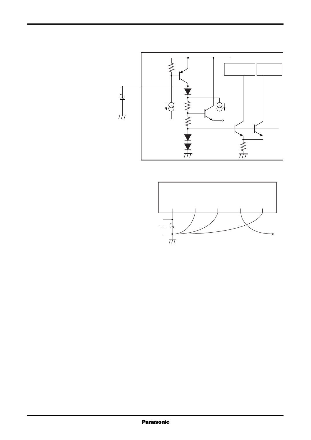
4. Ripple filter (continued)
6) After the power supply is
turned off (STB-low), it takes
15 kΩ
less than 10 seconds for the
total circuit current to become
12
the standby current (under 10
µA). If approx. 47 ohms resis-
tor is inserted between the
33 µF
350 µA
ripple filter terminal and GND
for the purpose of reducing
the inspection time with set, a
time until the current becomes
the standby current can be
shortened.
VCC
Constant
current source
Protection
circuit
10 kΩ
10 kΩ
1.7 mA
VREF
4 kΩ
Figure 5
5. GND terminal
1) Be sure to short-circuit each GND terminal of
pin 3, 8, 9 and 14 at the outside of the IC in use.
AN7198Z, AN7199Z
2) For each GND terminal, the one-point earth,
referenced to the GND connection point of
electrolytic capacitor between the supply ter-
1
3
8
9
14
minal and GND, is most effective for reduc-
ing the distortion. Even in the worst case,
ground pin 8, 9 of input GND separately from
all the other GND terminals.
Figure 6
To GND of input
3) Each GND terminal is not electrically short-circuited inside. Only pin 8 is connected with substrate.
4) Pin 9 is input signal GND. Connect only pin 9 with Pre-GND.
6. Cooling fin
1) The cooling fin is not connected with GND terminal by using Au wire. Only pin 8 is electrically connected
through substrate.
2) Always attach an outside heat sink to the cooling fin. The cooling fin must be fastened onto a chassis for use.
Otherwise, IC lead failure may occur.
3) Do not give the cooling fin any potential other than the GND potential. Otherwise, it may cause breakdown.
4) Connection of the cooling fin with GND can reduce the incoming noise hum. (It is unnecessary to connect
with GND in use, but connect with the power GND when the cooling fin is connected with GND)
7. Shock noise
1) STB on/off
No shock noise is released. However, the changeover switch of the standby terminal may make a slight
shock noise. In such a case, insert a capacitor of approx. 0.01 µF between the standby terminal and GND.
2) Mute on/off
No shock noise is released. Refer to the section on the mute function.
13
Share Link: 