AN7818F 查看數據表(PDF) - Panasonic Corporation
零件编号
产品描述 (功能)
生产厂家
AN7818F Datasheet PDF : 8 Pages
| |||
s Electrical Characteristics (Ta=25˚C)
· AN7815/7815F (15V Type)
Parameter
Symbol
Condition
min typ max Unit
Output voltage
Output voltage tolerance
VO
Tj=25˚C
14.4
15 15.6
V
VO
VI=18 to 30V, IO=5mA to 1A,
Tj=0 to 125˚C, PD =<*
14.25
15.75
V
Line regulation
REGIN
VI=17.5 to 30V, Tj=25˚C
VI=20 to 26V, Tj=25˚C
11 300 mV
3 150 mV
Load regulation
REGL
IO=5mA to 1.5A, Tj=25˚C
IO=250 to 750mA, Tj=25˚C
12 300 mV
4 150 mV
Bias current
Input bias current change
Load bias current change
Output noise voltage
Ibias
∆Ibias (IN)
∆Ibias (L)
Vno
Tj=25˚C
VI=17.5 to 30V, Tj=25˚C
IO=5mA to 1A, Tj=25˚C
f=10Hz to 100kHz
4
8 mA
1 mA
0.5 mA
90
µV
Ripple rejection ratio
RR
VI=18.5 to 28.5V, f=120Hz
54
dB
Minimum input/output voltage difference
Output impedance
VDIF (min.)
ZO
IO=1A, Tj=25˚C
f=1kHz
2
V
19
mΩ
Output short circuit current
IO (Short)
VI=30V, Tj=25˚C
700
mA
Peak output current
Output voltage temperature coefficient
IO (Peak)
∆VO/Ta
Tj=25˚C
IO=5mA, Tj=0 to 125˚C
2
A
–1
mV/˚C
Note 1) The specified condition Tj=25˚C means that the test should be carried out with the test time so short (within 10ms) that the
drift in characteristic value due to the rise in chip junction temperature can be ignored.
Note 2) When not specified, VI=23V, IO=500mA, CI=0.33µF and CO=0.1µF.
* AN7800 Series:15W, AN7800F Series:10.25W
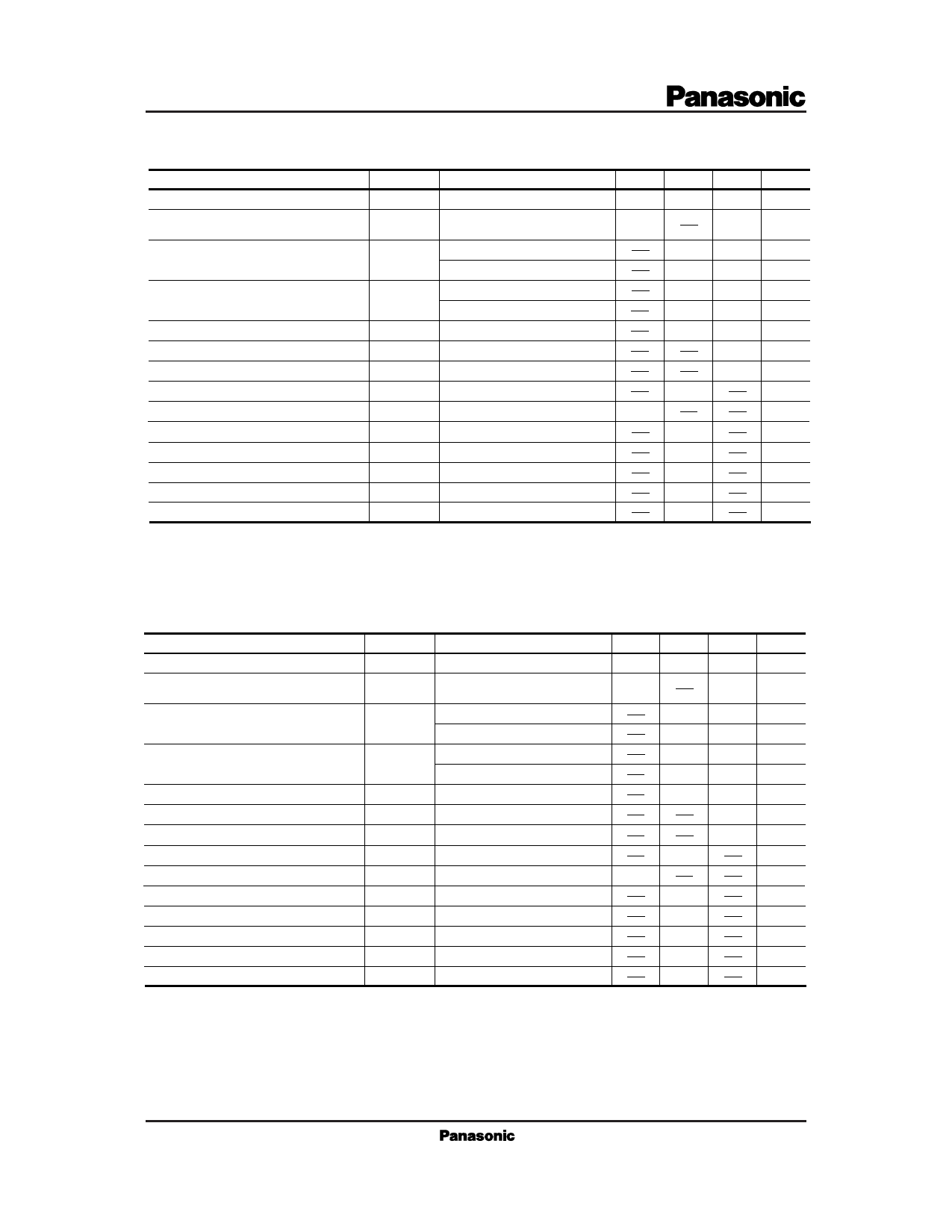
· AN7818/7818F (18V Type)
Parameter
Symbol
Condition
min typ max Unit
Output voltage
Output voltage tolerance
Line regulation
VO
Tj=25˚C
17.3
18 18.7
V
VO
VI=21 to 33V, IO=5mA to 1A,
Tj=0 to 125˚C, PD =< *
17.1
18.9
V
REGIN
VI=21 to 33V, Tj=25˚C
VI=24 to 30V, Tj=25˚C
14 360 mV
4 180 mV
Load regulation
REGL
IO=5mA to 1.5A, Tj=25˚C
IO=250 to 750mA, Tj=25˚C
12 360 mV
4 180 mV
Bias current
Ibias
Tj=25˚C
4.1
8 mA
Input bias current change
Load bias current change
Output noise voltage
∆Ibias (IN)
∆Ibias (L)
Vno
VI=21 to 33V, Tj=25˚C
IO=5mA to 1A, Tj=25˚C
f=10Hz to 100kHz
1 mA
0.5 mA
110
µV
Ripple rejection ratio
RR
VI=22 to 32V, IO=100mA, f=120Hz
53
dB
Minimum input/output voltage difference
Output impedance
VDIF (min.)
ZO
IO=1A, Tj=25˚C
f=1kHz
2
V
16
mΩ
Output short circuit current
IO (Short)
VI=35V, Tj=25˚C
700
mA
Peak output current
Output voltage temperature coefficient
IO (Peak)
∆VO/Ta
Tj=25˚C
IO=5mA, Tj=0 to 125˚C
2
A
–1.1
mV/˚C
Note 1) The specified condition Tj=25˚C means that the test should be carried out with the test time so short (within 10ms) that the
drift in characteristic value due to the rise in chip junction temperature can be ignored.
Note 2) When not specified, VI=27V, IO=500mA, CI=0.33µF and CO=0.1µF.
* AN7800 Series:15W, AN7800F Series:10.25W
Share Link: 