APA2177(2012) 查看數據表(PDF) - Anpec Electronics
零件编号
产品描述 (功能)
生产厂家
APA2177 Datasheet PDF : 20 Pages
| |||
APA2177
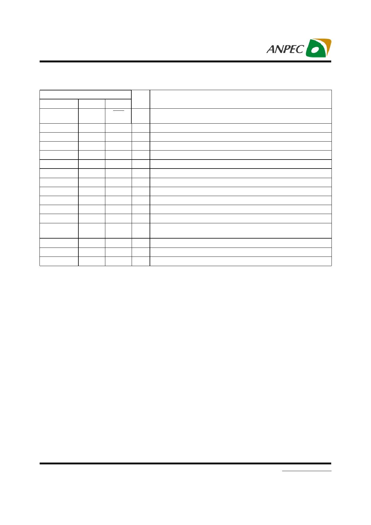
Pin Description
PIN
WLCS
P
A1
Name
SDN
A2
VDD
A3
LOUT
A4
LIN-
B1
GND
B2
CPP
B3
HPVDD
B4
LIN+
C1
CPN
C2
HPVSS
C3
SGND
C4
RIN+
D1
HI-Z
D2
GAIN
D3
ROUT
D4
RIN-
I/O/P
Function Description
I
Shutdown mode control pin. A low-level voltage applied on this pin shuts off the headphone driver.
P
Supply voltage input pin.
O Left channel output for headphone.
I
Left channel audio signal inverting input pin.
P
Ground connection for circuitry.
P
Charge pump flying capacitor positive connection.
P
Positive power supply for headphone amplifiers.
I
Left channel audio signal non-inverting input pin.
P
Charge pump flying capacitor negative connection.
P
Charge pump output.
I
Amplifier reference voltage.
I
Right channel audio signal non-inverting input pin.
Output impedance select. Set to logic LOW for normal operation and logic HIGH for high output
I
impedance.
I
Gain select. Set to logic LOW for a gain of 0dB and to HIGH for a gain of 6dB.
O Right channel output for headphone.
I
Right channel audio signal inverting input pin.
Copyright © ANPEC Electronics Corp.
5
Rev. A.1 - Jul., 2012
www.anpec.com.tw
Share Link: 