APW717818QBI-TRG 查看數據表(PDF) - Anpec Electronics
零件编号
产品描述 (功能)
生产厂家
APW717818QBI-TRG Datasheet PDF : 16 Pages
| |||
APW7178
Application Information (Cont.)
Output Capacitor Selection (Cont.)
IL
IP-FET
IPEAK
IOUT
ILIM
∆IL
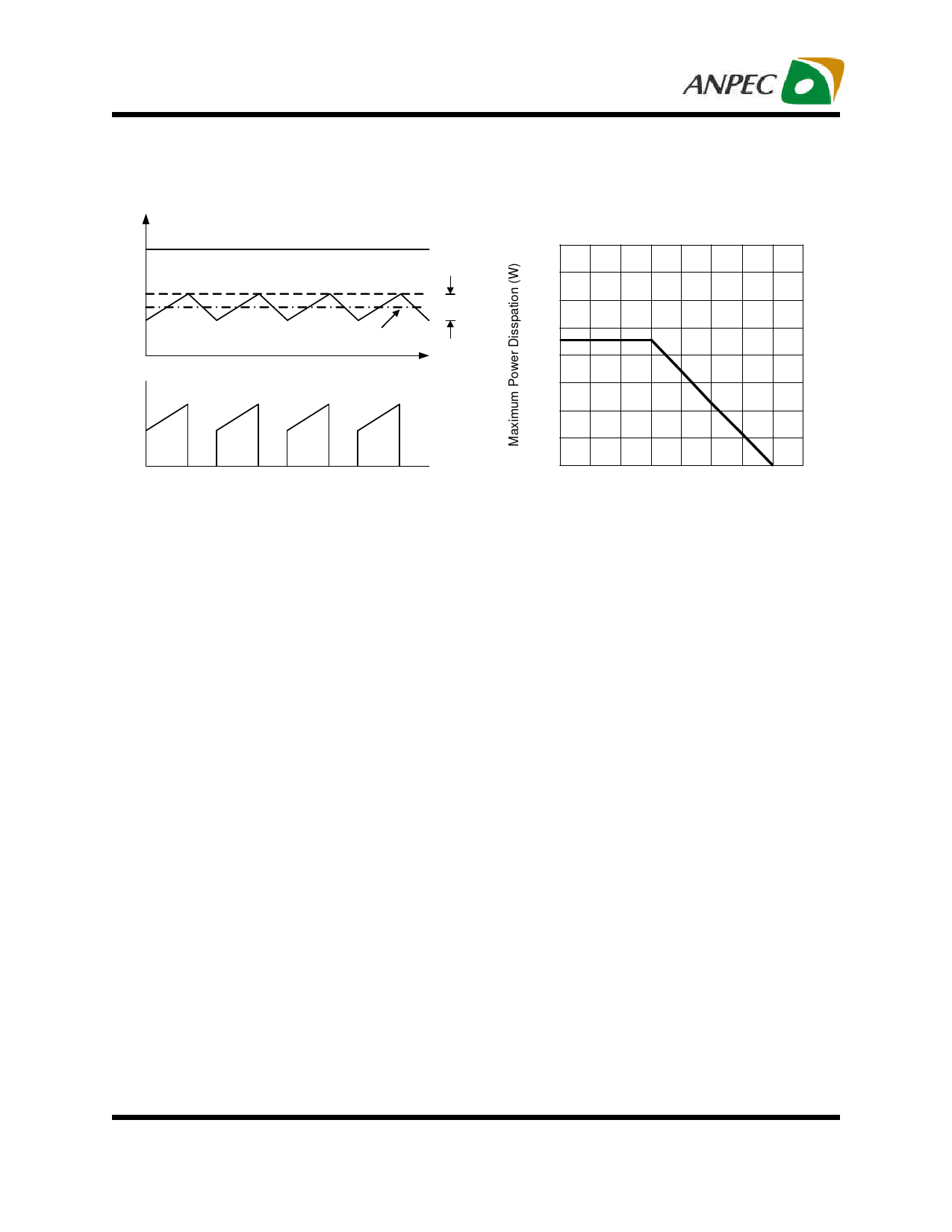
Thermal Consideration
In most applications, the APW7178 does not dissipate
much heat due to its high efficiency. But, in applications
where the APW7178 is running at high ambient tempera-
ture with low supply voltage and high duty cycles, the heat
dissipated may exceed the maximum junction tempera-
ture of the part. If the junction temperature reaches ap-
proximately 150°C, both power switches will be turned
off and the SW node will become high impedance.
To avoid the APW7178 from exceeding the maximum junc-
tion temperature, the user will need to do some thermal
analysis. The goal of the thermal analysis is to deter-
mine whether the power dissipated exceeds the maxi-
mum junction temperature of the part. The power dissi-
pated by the part is approximated:
PD
≅
I2
OUT
x
(RP-FET
x
D+RN-FET
x
(1-D))
The temperature rise is given by:
TR = (PD)(θJA)
Where P is the power dissipated by the regulator, D is
D
duty cycle of main switch
D = VOUT/VIN
The θJA is the thermal resistance from the junction of the
die to the ambient temperature. The junction temperature,
TJ, is given by:
T =T +T
J
A
R
Where TA is the ambient temperature.
The maximum power dissipation on the device can be
shown as the following figure:
0.8
0.7
0.6
0.5
0.4
0.3
0.2
0.1
0
-50 -25 0 25 50 75 100 125 150
Junction Temperature (oC)
Layout Consideration
For all switching power supplies, the layout is an impor-
tant step in the design; especially at high peak currents
and switching frequencies. If the layout is not carefully
done, the regulator might show noise problems and duty
cycle jitter.
1. The input capacitor should be placed close to the VIN
and GND. Connecting the capacitor and VIN/GND with
short and wide trace without any via holes for good
input voltage filtering. The distance between VIN/GND
to capacitor less than 2mm respectively is
recommended.
2. To minimize copper trace connections that can inject
noise into the system, the inductor should be placed
as close as possible to the SW pin to minimize the
noise coupling into other circuits.
3. The output capacitor should be place closed to VOUT
and GND.
4. Since the feedback pin and network is a high imped-
ance circuit the feedback network should be routed
away from the inductor. The feedback pin and feed-
back network should be shielded with a ground plane
or trace to minimize noise coupling into this circuit.
5. A star ground connection or ground plane minimizes
ground shifts and noise is recommended.
Copyright © ANPEC Electronics Corp.
11
Rev. A.2 - Jan., 2011
www.anpec.com.tw
Share Link: 