APX9270 查看數據表(PDF) - Anpec Electronics
零件编号
产品描述 (功能)
生产厂家
APX9270 Datasheet PDF : 17 Pages
| |||
APX9270
Function Description (Cont.)
Current Limit (Cont.)
recommended to short RL resistance and remove CM ca-
pacitor to disable external current limiter because the
internal current limiter is sufficient to avoid overload.
FG Output
The FG pin is an open drain output connecting a pull up
resistor to a high level voltage for the speed detection
function. When VIN- is larger than VIN+, the VFG is low (switch
on); when VIN- is smaller than VIN+, the VFG is high (switch
off). Leave it open when not in using.
Thermal Protection
The APX9270 is designed with a thermal protection to
protect the IC from the damage of over temperature.
When internal junction temperature reaches 160°C, the
output devices will be switched off. When the IC’s junc-
tion temperature cools by 20°C, the thermal sensor will
turn the output devices on again resulting in a pulsed
output during continuous thermal overload.
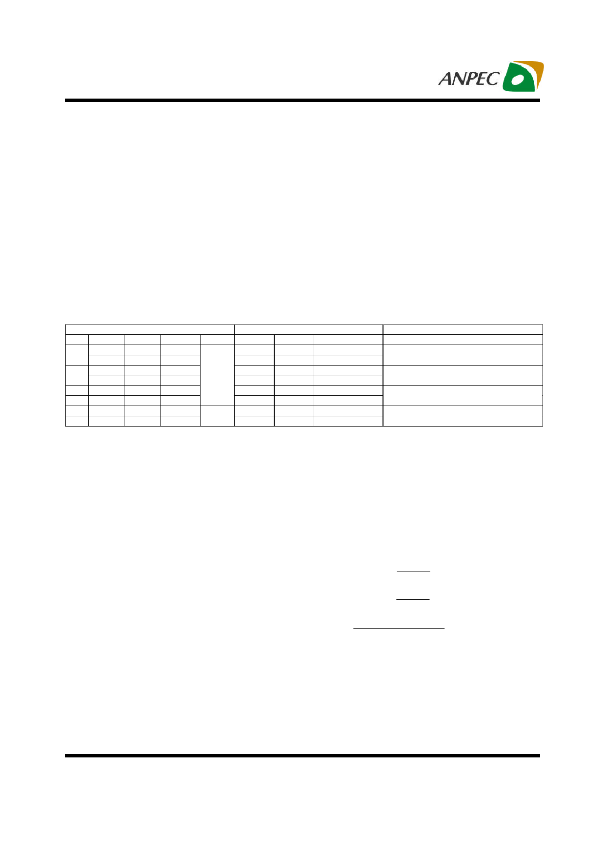
Truth Table
SET PWM
L
L
L
H
L
L
-
H
-
H
-
-
-
-
Input
IN-
IN+
H
L
L
H
H
L
L
H
H
L
L
H
H
L
L
H
Output
CT OUT1 OUT2
FG
H
L
L
L
H
OFF
L
OFF
L
L
OFF
L
OFF
OFF
L
L
L
OFF
OFF
H
OFF
L
L
OFF
L
OFF
Mode
Rotation (Drive)
Rotation (Regeneration)
Output Regeneration Mode by External
Signal
Lock Mode
SET or PWM=[L], “L” means that SET or PWM voltage is smaller than OSC voltage.
Also, SET or PWM=[H], “H” means that SET or PWM voltage is greater than OSC voltage.
Application Information
Input Protection Diode & Capacitor
The input protection diode (D1) between supply voltage
and VCC pin has to be used to prevent the reverse current
flowing into the supply power. However, the protection
diode will cause a voltage drop on the supply voltage.
The current rating of the diode must be larger than the
maximum output current. For the noise reduction purpose,
a capacitor (C1/CM) must be connected between VCC/VM
and SGND/PGND. The C1/C should be placed near the
M
device VCC/VM pin as close as possible.
Setting of the Oscillator Frequency and Output Voltage
The oscillator is used for PWM speed control. Compare
the OSC and SET pin voltages can decide PWM duty and
PWM frequency depends on the oscillator frequency. The
oscillator is based on internal charge/discharge circuit.
The circuit charges COSC to VOSCH by a 10µA source current,
and then it will discharge COSC to VOSCL by 10µA sink
current. The circuit can generate a triangular waveform.
The triangular waveform is determinded by COSC, R2, R3,
R4, and R4. (see Typical Application Circuit)
VOSCH = V6VREG × R3
R2 + R3
VOSCL = V6VREG × R5
R4 + R5
fOSC =
0.5 ×ISOC1
(VOSCH − VOSCL) × COSC
For example:
C =100pF,
OSC
R2
=
R5
=
10kΩ,
R3 = R4 = 20kΩ, IOSC1=10µA
VOSCH= 4V, VOSCL= 2V, fOSC=25kHz
The recommended OSC frequency range is from 22kHz
to 32kHz.
Copyright © ANPEC Electronics Corp.
11
Rev. A.3 - Jun., 2008
www.anpec.com.tw
Share Link: 