AS1506-BTDT-10 查看數據表(PDF) - austriamicrosystems AG
零件编号
产品描述 (功能)
生产厂家
AS1506-BTDT-10
austriamicrosystems AG

AS1506-BTDT-10 Datasheet PDF : 17 Pages
| |||
AS1506
Datasheet - Detailed Description
Copy Wiper Register to Non-Volatile Register
This command can be implemented as an 8- or 16-bit command. The data stored in the wiper register are transferred
to the non-volatile memory, to keep the data during power-down. There is no automatic trigger of this command during
power-down of the device. This command must be triggered before powering down the device.
There is a write non-volatile register time defined in the timing specification, which is required for storing the data in the
non-volatile register. During this time the device must not be powered down, otherwise the data stored in the non-vola-
tile register is corrupted.
Copy Non-Volatile Register to Wiper Register
This command can be implemented as an 8- or 16-bit command. The data stored in the non-volatile register are trans-
ferred to the wiper register, the wiper register moves to the stored position. This command is automatically executed
during power up of the system.
Read Non-Volatile Register
The AS1506 features the capability to read the data from the non-volatile register via the SPI interface (see Figure 23
on page 12). This command can be implemented as an 8- or 16-bit command. The SDIO pin is a bi-directional pin.
During the CSN low phase of the sequence the SDIO pin is used as input pin to set the command byte. After CSN ris-
ing edge the pin SDIO is set as output pin, the data stored in the non-volatile register are read serially, MSB first.
The data propagation starts at the second rising edge of SCLK after the rising edge of CSN. CSN must be high during
the read operation. With the next falling edge of CSN the SDIO pin is set to an input pin again.
Read Wiper Register
The AS1506 features the capability to read the data from the wiper register via the SPI interface (see Figure 23 on
page 12). This command can be implemented as an 8- or 16-bit command. The SDIO pin is a bi-directional pin. During
the CSN low phase of the sequence, the SDIO pin is used as input pin to set the command byte. After CSN rising edge
the pin SDIO is set as output pin, the data stored in the wiper register are read serially, MSB first. The wiper position is
unchanged.
The data propagation starts at the second rising edge of SCLK after the rising edge of CSN. CSN must be high during
the read operation. With the next falling edge of CSN the SDIO pin is set to an input pin again.
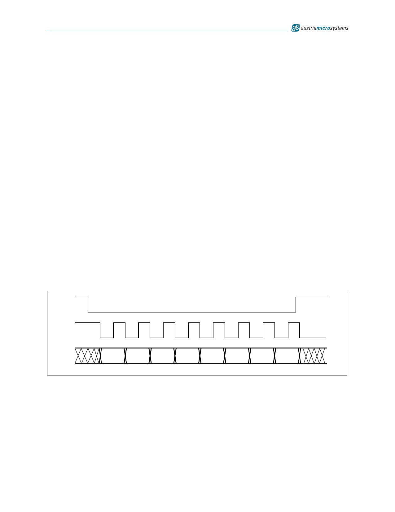
Figure 21. 8-Bit Command Word
CSN
SCLK
SDIO
C7
C6
C5
C4
C3
C2
C1
C0
www.austriamicrosystems.com
Revision 1.02
11 - 17
Share Link: