AS1520 查看數據表(PDF) - austriamicrosystems AG
零件编号
产品描述 (功能)
生产厂家
AS1520 Datasheet PDF : 29 Pages
| |||
AS1520/AS1521
Data Sheet - Electrical Characteristics
6 Electrical Characteristics
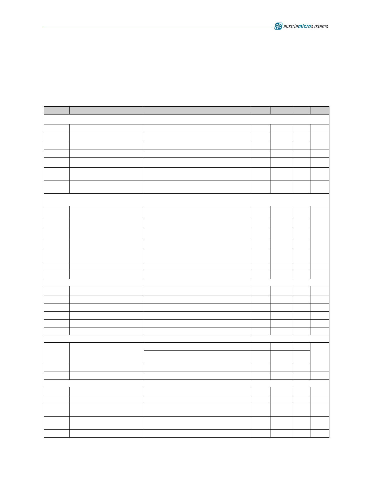
AS1520 Electrical Characteristics
VDD1 = VDD2 = VDD3 = +4.5 to +5.5V, COM = GND, fSCLK= 6.4MHz, 50% duty cycle, 16 clocks/conversion cycle
(400ksps), external +2.5V at REF, REFADJ = VDD1, TAMB = TMIN to TMAX (unless otherwise specified). Typ values at
TAMB = +25ºC.
Table 3. AS1520 Electrical Characteristics
Symbol
Parameter
Conditions
Min Typ Max Units
DC Accuracy 1
Resolution
10
Bits
INL
Relative Accuracy 2
-0.5
+0.5 LSB
DNL
Differential Nonlinearity
No missing codes over temperature
-1
+1 LSB
Offset Error
-3
+3 LSB
Gain Error 3
-3
+3 LSB
Gain-Error Temperature
Coefficient
±1.6
ppm/
°C
Channel-to-Channel
Offset Error Matching
±0.2
LSB
Dynamic Specifications: 100kHz sinewave input, 2.5Vp-p, 400ksps, 6.4MHz clock, bit RANGE (page 15) = 0,
pseudo-differential input mode
SINAD
Signal-to-Noise plus
Distortion Ratio
60
dB
THD Total Harmonic Distortion
Up to the 5th harmonic
70
dB
SFDR
Spurious-Free
Dynamic Range
70
dB
IMD Intermodulation Distortion
fIN1 = 99kHz, fIN2 = 102kHz
76
dB
Channel-to-Channel
Crosstalk 4
fIN = 200kHz, VIN = 2.5Vp-p
-85
dB
Full-Power Bandwidth
-3dB point
6
MHz
Full-Linear Bandwidth
SINAD > 68dB
450
kHz
Conversion Rate
tCONV
Conversion Time 5
2.5
µs
tACQ Track/Hold Acquisition Time
390 ns
tAD
Aperture Delay
7
ns
tAJ
Aperture Jitter
<50
ps
fSCLK
Serial Clock Frequency
0.5
6.4 MHz
Duty Cycle
40
60 %
Analog Inputs: CH0:CH7, COM
VCHx -
VCHy
(COM)
Input Voltage Range: Single-
Ended, Pseudo-Differential,
and Differential 6
Bit RANGE (page 15) = 1
Bit RANGE (page 15) = 0
0
-VREF
/2
VREF
+VREF V
/2
Multiplexer Leakage Current On/off leakage current, VCHx = 0 or VDD1 -1 ±0.001 +1 µA
Input Capacitance
18
pF
Internal Reference
VREF
TCVREF
CBYPREF
REF Output Voltage
REF Short-Circuit Current
REF Output Temperature
Coefficient
Load Regulation 7
Capacitive Bypass at REF
TAMB = +25ºC
0 to 1mA output load
2.48 2.50 2.52 V
30
mA
±25
ppm/
°C
1.2
4.0
mV/
mA
4.7
10 µF
www.austriamicrosystems.com
Revision 1.00
5 - 29
Share Link: 