AS1701-T 查看數據表(PDF) - austriamicrosystems AG
零件编号
产品描述 (功能)
生产厂家
AS1701-T Datasheet PDF : 17 Pages
| |||
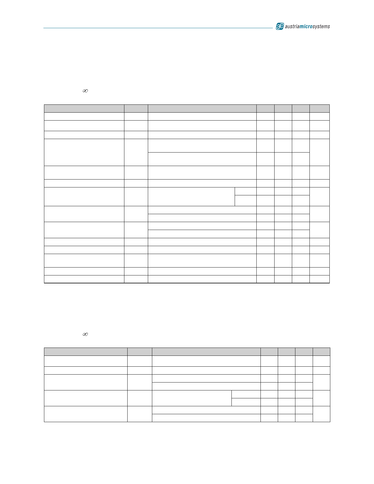
AS1701, AS1706
Data Sheet - Electrical Characteristics
6 Electrical Characteristics
All specifications are 100% tested at TAMB = +25ºC.
5V Operation
VDD = 5V, RL = ∞, CBIAS = 0.1µF to GND, SHDN = GND, TAMB +25ºC (unless otherwise specified).
Table 3. DC Electrical Characteristics – 5V Operation
Parameter
Supply Voltage Range
Supply Current 1
Shutdown Supply Current
SHDN Threshold
Common-Mode Bias Voltage 2
Output Offset Voltage
Power Supply Rejection Ratio
Output Power 3
Total Harmonic
Distortion+Noise
Thermal-Shutdown Threshold
Thermal-Shutdown Hysteresis
Power-Up/Enable from
Shutdown Time
Shutdown Time
Turn-Off Transient
Symbol
VDD
IDD
ISHDN
VBIAS
VOS
PSRR
POUT
THD+N
tPU
tSHDN
VPOP
Conditions
Inferred from PSRR Test
TAMB = -40 to +85ºC
SHDN = VDD
VIH
VIL
Av = 2, IN- = OUT+, IN- = BIAS
Inputs Grounded, VRIPPLE = 217Hz
200mVp-p, RL = 4Ω, VIN- = VIN+ =
VBIAS
1kHz
RL = 4Ω, THD+N = 1%, fIN = 1kHz
RL = 8Ω, THD+N = 1%, fIN = 1kHz
AV = 2, RL = 4Ω, fIN = 1kHz, POUT = 1.3W
AV = 2, RL = 8Ω, fIN = 1kHz, POUT = 1W
Min Typ Max
2.7
5.5
6.8 10.4
0.01 1
VDD x
0.7
VDD x
0.3
VDD/2
- 5%
VDD/2
VDD/2
+ 5%
±1 ±10
65
63
1.6
0.8 1.2
0.09
0.05
145
9
150
1
20
Units
V
mA
µA
V
V
mV
dB
W
%
ºC
ºC
ms
µs
mV
1. Quiescent power supply current is specified and tested without loads on the outputs. Quiescent power supply
current depends on the offset voltage when a practical load is connected to the device.
2. Common-mode bias voltage is the voltage on pin BIAS and is nominally VDD/2.
3. Guaranteed by design.
3V Operation
VDD = 3V, RL = ∞, CBIAS = 0.1µF to GND, SHDN = GND, TAMB +25ºC (unless otherwise specified).
Table 4. DC Electrical Characteristics – 3V Operation
Parameter
Symbol
Conditions
Min Typ Max Units
Supply Current 1
IDD
TAMB = -40 to +85ºC
6 10 mA
Shutdown Supply Current
ISHDN
SHDN = VDD
0.01 1 µA
Output Power 2
POUT
RL = 4Ω, THD+N = 1%, fIN = 1kHz
RL = 8Ω, THD+N = 1%, fIN = 1kHz
0.6
W
0.4
Power Supply Rejection Ratio
PSRR
VRIPPLE = 200mVp-p,
RL = 8Ω, VIN- = VIN+ = VBIAS
217Hz
1kHz
65
dB
63
AV = 2, RL = 4Ω, fIN = 1kHz, POUT = 500mW
0.09
Total Harmonic Distortion +Noise THD+N
%
AV = 2, RL = 8Ω, fIN = 1kHz, POUT = 350mW
0.06
1. Quiescent power supply current is specified and tested without loads on the outputs. Quiescent power supply
current depends on the offset voltage when a practical load is connected to the device.
2. Guaranteed by design.
www.austriamicrosystems.com
Revision 1.52
4 - 17
Share Link: 