AS1741 查看數據表(PDF) - austriamicrosystems AG
零件编号
产品描述 (功能)
生产厂家
AS1741 Datasheet PDF : 15 Pages
| |||
AS1741, AS1742, AS1743
Data Sheet
austriamicrosystems
Power Supply Sequencing
9 Application Information
Power Supply Sequencing
Proper power-supply sequencing is critical for proper switch operation. The power supplies should be started up in the
following sequence:
1. V+
2. NOx, NCx, COMx
Note: Operation beyond the absolute maximum ratings (see page 2) may permanently damage the devices.
Power Supply Bypass
Power supply connections to the devices must maintain a low impedance to ground. This can be done using a bypass
capacitor, which will also improve noise margin and prevent switching noise propagation from the V+ supply to other
components.
A 0.1µF bypass capacitor, connected from V+ to GND (see Figure 17 on page 11), is adequate for most applications.
Logic Inputs
Driving INx Rail-to-Rail will help minimize power consumption.
Layout Considerations
High-speed switches require proper layout and design procedures for optimum performance.
! Short, wide traces should be used to reduce stray inductance and capacitance.
! Bypass capacitors should be as close to the device as possible.
! Large ground planes should be used wherever possible.
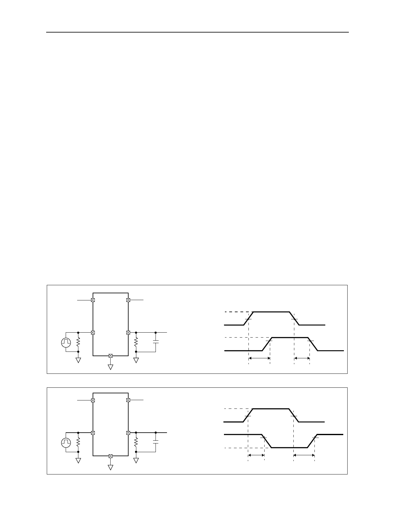
Timing Diagrams and Test Setups
Figure 12. AS1741/AS1743 Test Circuit and Timing Diagram
V+
V+
NOx
AS1741/
AS1743
INx
50Ω
COMx
GND
VNOx
50Ω
VCOMx
35pF
VIH + 0.5V
INx
0
VNOx
VCOMx
0
50%
90%
tON
tR < 5ns
tF < 5ns
50%
90%
tOFF
Figure 13. AS1742/AS1743 Test Circuit and Timing Diagram
V+
V+
NCx
AS1742/
AS1743
INx
50Ω
COMx
GND
VNCx
50Ω
VCOMx
35pF
VIH + 0.5V
INx
0
VNCx
VCOMx
0
50%
90%
tOFF
50%
tR < 5ns
tF < 5ns
90%
tON
www.austriamicrosystems.com
Revision 1.76
9 - 15
Share Link: 