AS1745 查看數據表(PDF) - austriamicrosystems AG
零件编号
产品描述 (功能)
生产厂家
AS1745 Datasheet PDF : 16 Pages
| |||
AS1744, AS1745
Data Sheet
austriamicrosystems
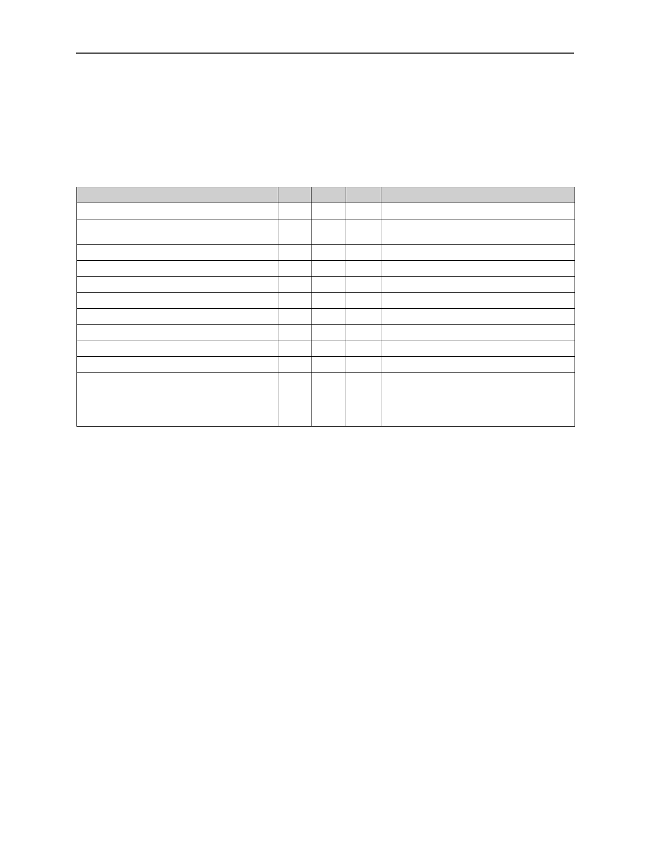
4 Absolute Maximum Ratings
Stresses beyond those listed in Table 1 may cause permanent damage to the device. These are stress ratings only,
and functional operation of the device at these or any other conditions beyond those indicated in Section 5 Electrical
Characteristics on page 3 is not implied. Exposure to absolute maximum rating conditions for extended periods may
affect device reliability.
Table 1. Absolute Maximum Ratings
Parameter
V+, IN1, IN2 to GND
Min Max Units
-0.3 +7
V
Comments
COMx, NOx, NCx to GND †
-0.3
COMx, NOx, NCx Continuous Current
-100
COMx, NOx, NCx Peak Current
-150
Continuous Power Dissipation (TAMB = +70ºC)
Electro-Static Discharge
Latch Up Immunity
Operating Temperature Range
-40
Junction Temperature
Storage Temperature Range
-65
Package Body Temperature
V+
+ 0.3
+100
+150
330
1000
100
+85
150
+150
+260
V
mA
mA
Pulsed at 1ms, 10% duty cycle
mW
Derate at 4.7mW/ºC above +70ºC
V
HBM Mil-Std883E 3015.7 methods
mA
Norm: JEDEC 17
ºC
ºC
ºC
The reflow peak soldering temperature (body
temperature) specified is in accordance with
ºC IPC/JEDEC J-STD-020C “Moisture/Reflow
Sensitivity Classification for Non-Hermetic
Solid State Surface Mount Devices”
† Signals on pins COM1, COM2, NO1, NO2, NC1, or NC2 that exceed V+ or GND are clamped by internal diodes.
Limit forward-diode current to the maximum current rating.
www.austriamicrosystems.com
Revision 1.53
2 - 16
Share Link: 