AS1744V-T 查看數據表(PDF) - austriamicrosystems AG
零件编号
产品描述 (功能)
生产厂家
AS1744V-T
austriamicrosystems AG

AS1744V-T Datasheet PDF : 16 Pages
| |||
AS1744, AS1745
Data Sheet
austriamicrosystems
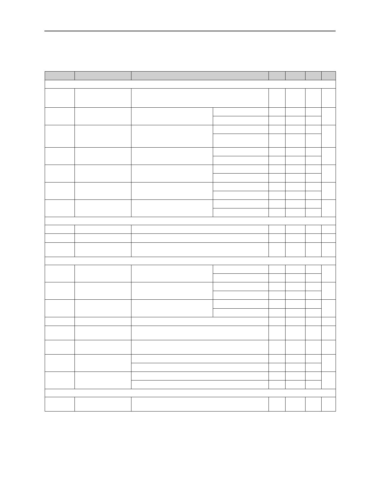
V+ = +2.7 to 3.6V, VIH = +2.0V, VIL = +0.4V, TAMB = TMIN to TMAX (unless otherwise specified). Typ values @ TAMB = +25ºC.
Table 3. +3V Supply Electrical Characteristics
Symbol
Parameter
Analog Switch
VCOMx,
VNOx,
VNCx
Analog Signal Range
Conditions
Min Typ Max Unit
0
V+ V
RON
ON-Resistance
V+ = 2.7V, ICOMx = 10mA,
VNOx or VNCx = 0 to V+
TAMB = +25ºC
TAMB = TMIN to TMAX
5 5.5
Ω
8
∆RON
ON-Resistance
Match Between
Channels 1
V+ = 2.7V, ICOMx = 10mA,
VNOx or VNCx = 0 to V+
TAMB = +25ºC
TAMB = TMIN to TMAX
0.1 0.2
Ω
0.4
RFLAT(ON)
ON-Resistance
Flatness 2
V+ = 2.7V, ICOMx = 10mA,
VNOx or VNCx = 0 to V+
TAMB = +25ºC
TAMB = TMIN to TMAX
1.5 2
Ω
2.5
INOx(OFF), NOx or NCx Off-
INCx(OFF) Leakage Current 3
V+ = 3.3V, VCOMx = 1 or 3V,
VNOx or VNCx = 3 or 1V
TAMB = +25ºC
-0.1 ±0.01 0.1
TAMB = TMIN to TMAX -0.3
0.3
nA
COMx Off-Leakage
ICOMx(OFF)
Current 3
V+ = 3.3V, VCOMx = 1 or 3V,
VNOx or VNCx = 3 or 1V
TAMB = +25ºC
-0.1 ±0.01 0.1
TAMB = TMIN to TMAX -3
3
nA
COMx On-Leakage
ICOMx(ON)
Current 3
Logic Input: (INx)
V+ = 3.3V, VCOMx = 1 or 3V,
VNOx or VNCx = 1 or 3V
TAMB = +25ºC
-0.4
TAMB = TMIN to TMAX -4
±0.1
0.4
4
nA
VIH
Input Logic High
2.0
V
VIL
Input Logic Low
0.4 V
IIH,IIL
Input Leakage
Current
Switch Dynamic Characteristics
VINx = 0 or +5.5V
-100 5 100 nA
tON
Turn On Time 3
VNOx or VNCx = 2V, RLOAD =
TAMB = +25ºC
300Ω, CLOAD = 35pF, Figure 11 TAMB = TMIN to TMAX
17 23
ns
28
tOFF
Turn Off Time 3
VNOx or VNCx = 2V, RLOAD =
TAMB = +25ºC
300Ω, CLOAD = 35pF, Figure 11 TAMB = TMIN to TMAX
6
8
ns
10
tBBM
Break-Before-Make 3
VNOx or VNCx = 2V, RLOAD =
300Ω, CLOAD = 35pF, Figure 12
TAMB = +25ºC
TAMB = TMIN to TMAX
1
11
ns
Q
Charge Injection
VGEN = 1.5V, RGEN = 0, CLOAD = 1.0nF, Figure 13
0
pC
CNOx(OFF),
CNCx(OFF)
NOx, NCx Off-
Capacitance
VNOx or VNCx = GND, f = 1MHz, Figure 14
20
pF
CCOMx(ON)
COMx On-
Capacitance
VCOMx = GND, f = 1MHz, Figure 14
56
pF
VISO
Off-Isolation 4
f = 10MHz, RLOAD = 50Ω, CLOAD = 5pF, Figure 15
f = 1MHz, RLOAD = 50Ω, CLOAD = 5pF, Figure 15
-52
dB
-85
VCT
Crosstalk 5
Power Supply
f = 10MHz, RLOAD = 50Ω, CLOAD = 5pF, Figure 15
f = 1MHz, RLOAD = 50Ω, CLOAD = 5pF, Figure 15
-52
dB
-90
I+
Positive Supply
Current
V+ = 3.6V, VIN = 0 or +3.6V
0.01 1.0 µA
1. ∆RON = RON(MAX) - RON(MIN).
2. Flatness is defined as the difference between the maximum and the minimum value of ON-resistance as measured
over the specified analog signal ranges.
3. Guaranteed by design.
4. Off-Isolation = 20log10(VCOMx/VNOx), VCOMx = output, VNOx = input to off switch.
5. Between any two switches.
www.austriamicrosystems.com
Revision 1.53
4 - 16
Share Link: