AS1745V-T 查看數據表(PDF) - austriamicrosystems AG
零件编号
产品描述 (功能)
生产厂家
AS1745V-T
austriamicrosystems AG

AS1745V-T Datasheet PDF : 16 Pages
| |||
AS1744, AS1745
Data Sheet
austriamicrosystems
Power-Supply Sequencing
8 Application Information
Power-Supply Sequencing
Proper power-supply sequencing is critical for proper operation. The recommended sequence is as follows:
1. V+
2. NOx, NCx, COMx
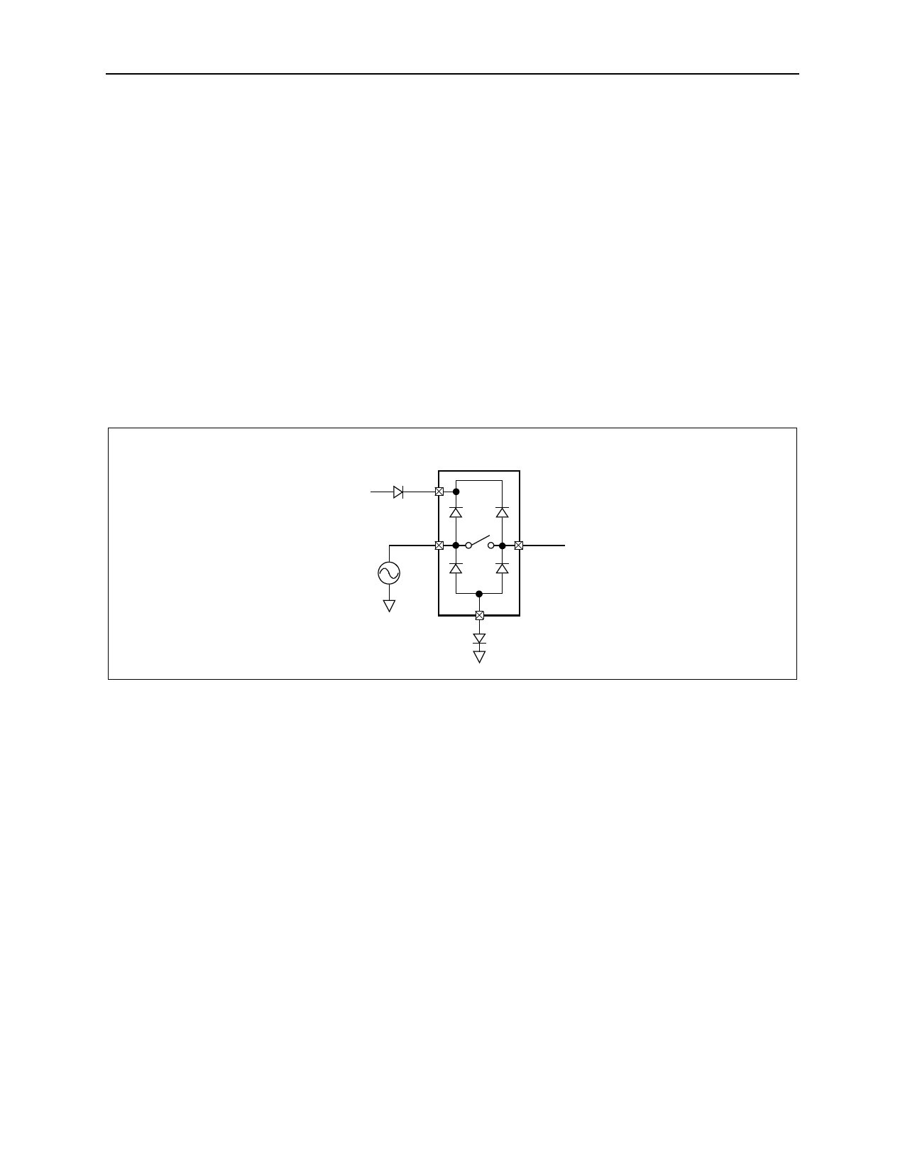
Always apply V+ before applying analog signals, especially if the analog signal is not current-limited. If the above
sequence is not possible, and if the analog inputs are not current-limited to less than 30mA, add a small-signal diode
as shown in Figure 10 (D1). If the analog signal can dip below GND, add diode D2. Adding these diodes will reduce the
analog range to a diode-drop (about 0.7V) below V+ (for D1), and a diode-drop above ground (for D2).
Note: Operation beyond the absolute maximum ratings (see page 2) may permanently damage the devices.
Overvoltage Protection
ON-resistance increases slightly at lower supply voltages.
Figure 10. Overvoltage Protection Using 2 External Blocking Diodes
AS1744/AS1745
V+ D1 V+
NOx
VGEN
COMx
GND
D2
Adding diode D2 to the circuit shown in Figure 10 causes the logic threshold to be shifted relative to GND. Diodes D1
and D2 also protect against overvoltage conditions.
For example, in the circuit shown in Figure 10, if the supply voltage goes below the absolute maximum rating, and if a
fault voltage up to the absolute maximum rating is applied to an analog signal pin, no damage will result.
Note: The supply voltage (V+) must not exceed the absolute maximum rating of +7V.
Power Supply Bypass
Power supply connections to the devices must maintain a low impedance to ground. This can be done using a bypass
capacitor, which will also improve noise margin and prevent switching noise propagation from the V+ supply to other
components.
Layout Considerations
High-speed switches require proper layout and design procedures for optimum performance.
! Reduce stray inductance and capacitance by keeping traces short and wide.
! Ensure that bypass capacitors are as close to the device as possible.
! Use large ground planes where possible.
www.austriamicrosystems.com
Revision 1.53
7 - 16
Share Link: