AS1747(2009) 查看數據表(PDF) - austriamicrosystems AG
零件编号
产品描述 (功能)
生产厂家
AS1747
(Rev.:2009)
(Rev.:2009)
austriamicrosystems AG

AS1747 Datasheet PDF : 13 Pages
| |||
AS1747
Datasheet - Detailed Description
8 Detailed Description
The AS1747 operates from a +1.8V to +5.5V supply and features a negative signal capability that allows signals below
ground to pass through without distortion. A break-before-make switching and a low on-resistance is also included in
this analog dual SPDT switch. The device is fully specified for a 3.0V application.
9 Application Information
Digital Control Inputs
The logic inputs of the AS1747 accept up to +5.5V independent of the supply voltage. Due to this a mixing of the logic
levels in a system is possible. For example, with a +3.3V supply, IN_ can be driven low to GND and high to +5.5V. For
a +1.8V supply voltage, the logic levels are 0.5V (low) and 1.4V (high); for a +5V supply voltage, the logic levels are
0.8V (low) and 2.0V (high).
Analog Signal Levels
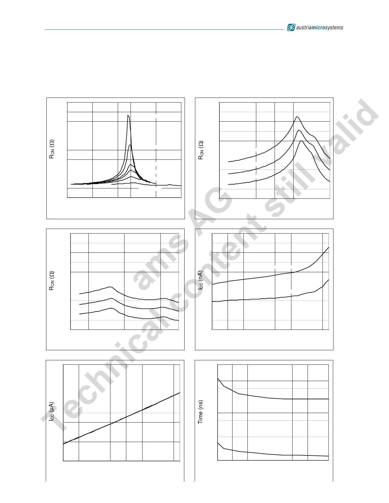
The change of the on-resistance of the AS1747 is very little for analog input signals over the whole supply voltage
range. The switches are bi-directional, so the NO_, NC_, and COM_ pins can be either inputs or outputs.
The AS1747 pass signals as low as VCC - 5.5V, including signals below ground with minimal distortion.
Power-Supply Sequencing and Overvoltage Protection
Caution: Do not exceed the absolute maximum ratings since stresses beyond the listed ratings may cause
permanent damage to the device.
Proper power-supply sequencing is recommended for all CMOS devices. Always apply VCC before applying analog
signals, especially if the analog signal is not current-limited.
www.austriamicrosystems.com
Revision 1.01
8 - 13
Share Link: