AS1753S 查看數據表(PDF) - austriamicrosystems AG
零件编号
产品描述 (功能)
生产厂家
AS1753S
austriamicrosystems AG

AS1753S Datasheet PDF : 16 Pages
| |||
AS1751/AS1752/AS1753
Data Sheet - Electrical Characteristics
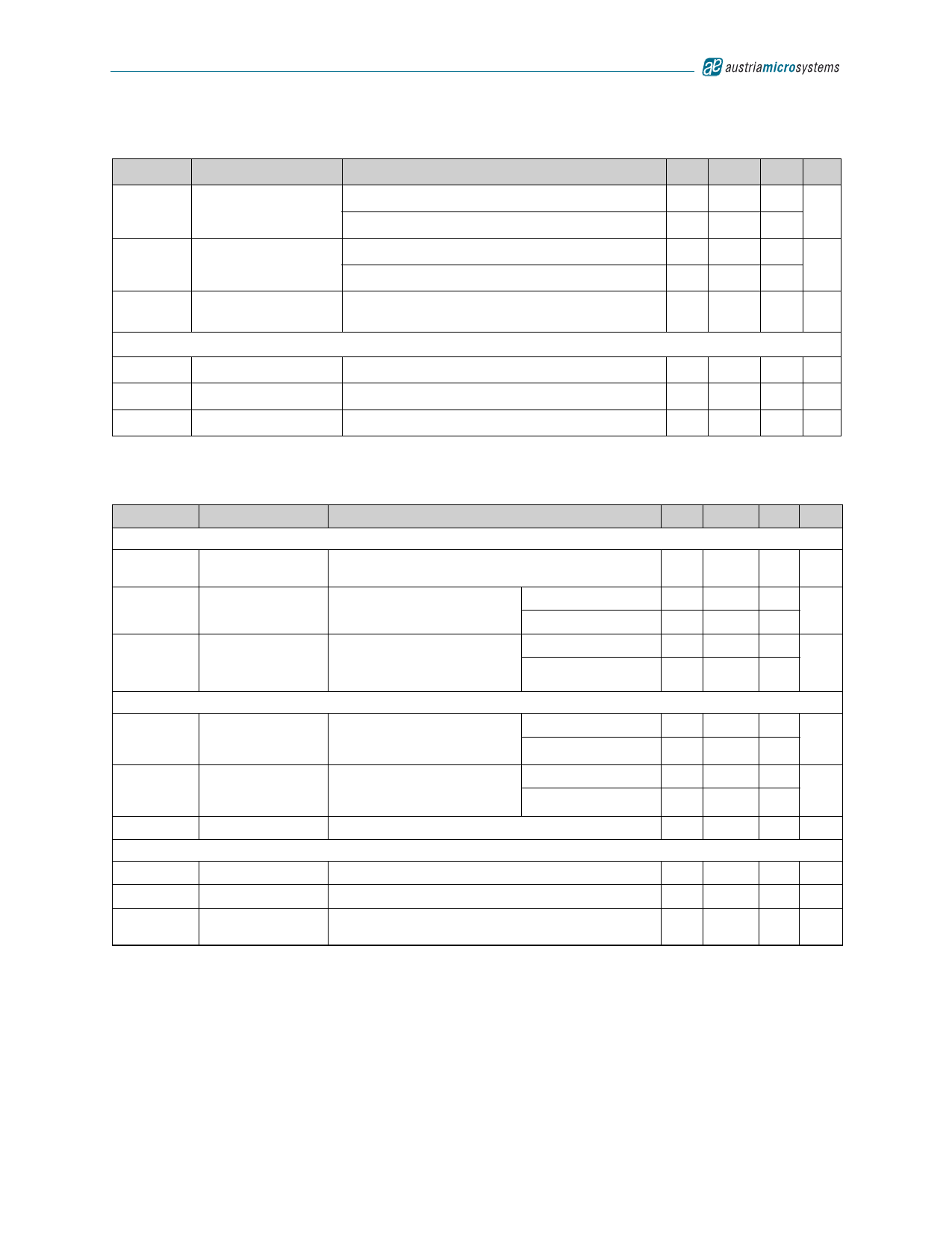
Table 4. +3V Supply Electrical Characteristics (Continued)
Symbol
Parameter
Conditions
Min Typ Max Unit
f = 10MHz, RLOAD = 50Ω, CLOAD = 5pF, Figure 18
-40
VISO
Off-Isolation 4
dB
f = 1MHz, RLOAD = 50Ω, CLOAD = 5pF, Figure 18
-55
f = 10MHz, RLOAD = 50Ω, CLOAD = 5pF, Figure 18
-70
Crosstalk 5
dB
f = 1MHz, RLOAD = 50Ω, CLOAD = 5pF, Figure 18
-80
THD
Total Harmonic
Distortion
f = 20Hz to 20kHz, VCOMx = 2Vp-p, RLOAD = 32Ω
0.033
%
Logic Input
VIH
Input Logic High
1.4
V
VIL
Input Logic Low
0.5 V
IIN
Input Leakage Current
VINx = 0 or V+
-1 0.0001 +1 µA
V+ = +1.8V, VIH = +1.0V, VIL = 0.4V, TAMB = TMIN to TMAX (unless otherwise specified). Typ values @ TAMB = +25ºC.
Table 5. +1.8V Supply Electrical Characteristics
Symbol
Parameter
Conditions
Min Typ Max Unit
Analog Switch
VCOMx,
VNOx, VNCx
Analog Signal
Range
0
V+ V
RON
ON-Resistance
V+ = 1.8V, ICOMx = 10mA,
VNOx or VNCx = 0.9V
TAMB = +25ºC
TAMB = TMIN to TMAX
0.9 2.5
Ω
3
ΔRON
ON-Resistance
Match Between
Channels 1
V+ = 1.8V, ICOMx = 10mA,
VNOx or VNCx = 0.9V
TAMB = +25ºC
TAMB = TMIN to TMAX
0.05 0.25
Ω
0.25
Switch Dynamic Characteristics
VNOx or VNCx = 1.0V,
TAMB = +25ºC
tON
Turn On Time 3
RLOAD = 50Ω, CLOAD = 35pF,
Figures 13, 14
TAMB = TMIN to TMAX
22 30
ns
35
tOFF
Turn Off Time 3
VNOx or VNCx = 1.0V,
TAMB = +25ºC
RLOAD = 50Ω, CLOAD = 35pF,
Figures 13, 14
TAMB = TMIN to TMAX
12 20
ns
25
Q
Charge Injection VGEN = V+, RGEN = 0, CLOAD = 1.0nF, Figure 16
1
pC
Logic Input
VIH
Input Logic High
1.0
V
VIL
Input Logic Low
0.4 V
IIN
Input Leakage
Current
VINx = 0 or V+
-1 0.0001 +1 µA
1. ΔRON = RON(MAX) - RON(MIN).
2. Flatness is defined as the difference between the maximum and the minimum value of ON-resistance as measured
over the specified analog signal ranges.
3. Guaranteed by design.
4. Off-Isolation = 20log10(VCOMx/VNOx), VCOMx = output, VNOx = input to off switch.
5. Between two switches.
www.austriamicrosystems.com
Revision 1.41
5 - 16
Share Link: