AS1910V-T 查看數據表(PDF) - austriamicrosystems AG
零件编号
产品描述 (功能)
生产厂家
AS1910V-T
austriamicrosystems AG

AS1910V-T Datasheet PDF : 15 Pages
| |||
AS1910 - AS1915
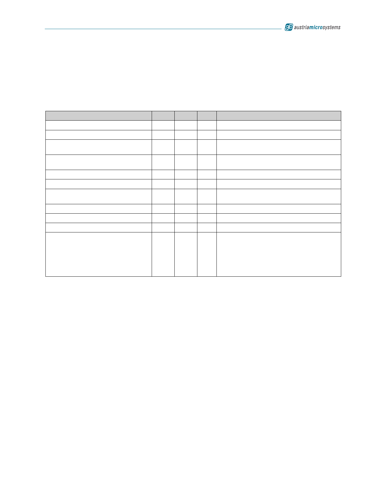
Data Sheet - Absolute Maximum Ratings
5 Absolute Maximum Ratings
Stresses beyond those listed in Table 3 may cause permanent damage to the device. These are stress ratings only,
and functional operation of the device at these or any other conditions beyond those indicated in Section 5 Electrical
Characteristics on page 3 is not implied. Exposure to absolute maximum rating conditions for extended periods may
affect device reliability.
Table 3. Absolute Maximum Ratings
Parameter
Min Max Units
Comments
VCC, VCC2 to GND
Open-Drain RESETN
-0.3 +5.0 V
-0.3 +7.0 V
Push/Pull RESET, RESETN
-0.3
VCC +
0.3
V
MRN, WDI, RESETIN to GND
-0.3
VCC +
0.3
V
Input Current (VCC)
Output Current (RESET, RESETN)
Continuous Power Dissipation
(TAMB = +70ºC)
Operating Temperature Range
20 mA
20 mA
696 mW
-40 +125 ºC
Derate 8.7mW/ºC above +70ºC
Junction Temperature
+150 ºC
Storage Temperature Range
Package Body Temperature
-65 +150 ºC
+260
The reflow peak soldering temperature (body
temperature) specified is in accordance with
IPC/JEDEC J-STD-020C “Moisture/Reflow
ºC Sensitivity Classification for Non-Hermetic Solid
State Surface Mount Devices”.
The lead finish for Pb-free leaded packages is
matte tin (100% Sn).
www.austriamicrosystems.com
Revision 1.00
3 - 15
Share Link: