25F1024AN 查看數據表(PDF) - Atmel Corporation
零件编号
产品描述 (功能)
生产厂家
25F1024AN Datasheet PDF : 20 Pages
| |||
The WRSR instruction also allows the user to enable or disable the Write Protect (WP) pin
through the use of the write protect enable (WPEN) bit. Hardware write protection is enabled
when the WP pin is low and the WPEN bit is “1”. Hardware write protection is disabled when
either the WP pin is high or the WPEN bit is “0.” When the device is hardware write protected,
writes to the Status Register, including the Block Protect bits and the WPEN bit, and the locked-
out sectors in the memory array are disabled. Write is only allowed to sectors of the memory
which are not locked out. The WRSR instruction is self-timed to automatically erase and pro-
gram BP0, BP1, and WPEN bits. In order to write the status register, the device must first be
write enabled via the WREN instruction. Then, the instruction and data for the three bits are
entered. During the internal write cycle, all instructions will be ignored except RDSR instructions.
The AT25F1024A will automatically return to write disable state at the completion of the WRSR
cycle.
Note: When the WPEN bit is hardware write protected, it cannot be changed back to “0”, as long as the
WP pin is held low.
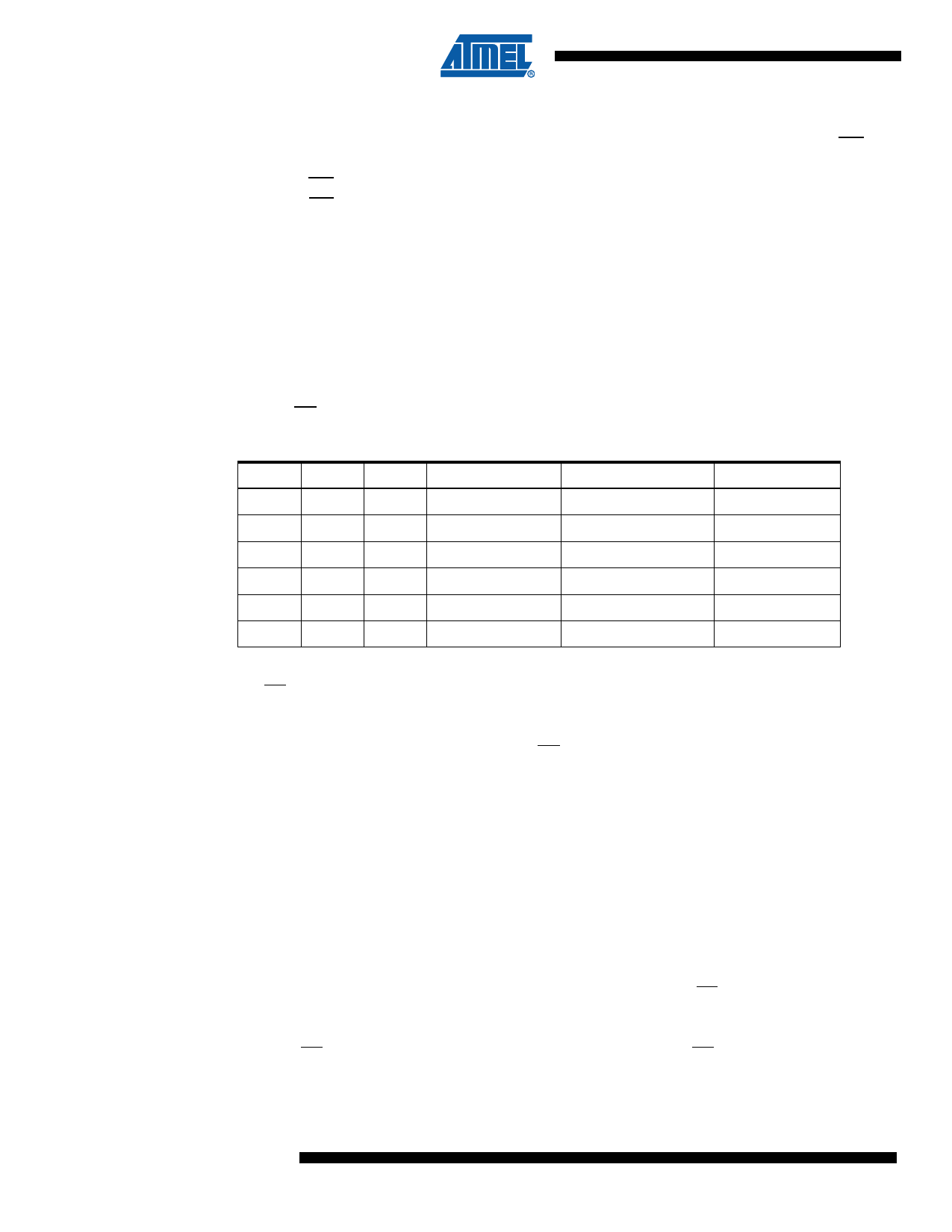
Table 2-5. WPEN Operation
WPEN WP WEN ProtectedBlocks
0
X
0
Protected
0
X
1
Protected
1
Low
0
Protected
1
Low
1
Protected
X
High
0
Protected
X
High
1
Protected
UnprotectedBlocks
Protected
Writable
Protected
Writable
Protected
Writable
Status Register
Protected
Writable
Protected
Protected
Protected
Writable
READ (READ): Reading the AT25F1024A via the SO pin requires the following sequence. After
the CS line is pulled low to select a device, the Read instruction is transmitted via the SI line fol-
lowed by the byte address to be read (see Table 3-6 on page 13). Upon completion, any data on
the SI line will be ignored. The data (D7-D0) at the specified address is then shifted out onto the
SO line. If only one byte is to be read, the CS line should be driven high after the data comes
out. The Read instruction can be continued since the byte address is automatically incremented
and data will continue to be shifted out. For the AT25F1024A, when the highest address is
reached, the address counter will roll over to the lowest address allowing the entire memory to
be read in one continuous Read instruction.
PROGRAM (PROGRAM): In order to program the AT25F1024A, two separate instructions must
be executed. First, the device must be write enabled via the WREN instruction. Then the Pro-
gram instruction can be executed. Also, the address of the memory location(s) to be
programmed must be outside the protected address field location selected by the Block Write
Protection Level. During an internal self-timed programming cycle, all commands will be ignored
except the RDSR instruction.
The Program instruction requires the following sequence. After the CS line is pulled low to select
the device, the Program instruction is transmitted via the SI line followed by the byte address
and the data (D7-D0) to be programmed (see Table 3-7 on page 14). Programming will start
after the CS pin is brought high. The low-to-high transition of the CS pin must occur during the
SCK low time immediately after clocking in the D0 (LSB) data bit.
10 AT25F1024A
3346G–SFLSH–7/07
Share Link: 