25F1024AN 查看數據表(PDF) - Atmel Corporation
零件编号
产品描述 (功能)
生产厂家
25F1024AN Datasheet PDF : 20 Pages
| |||
AT25F1024A
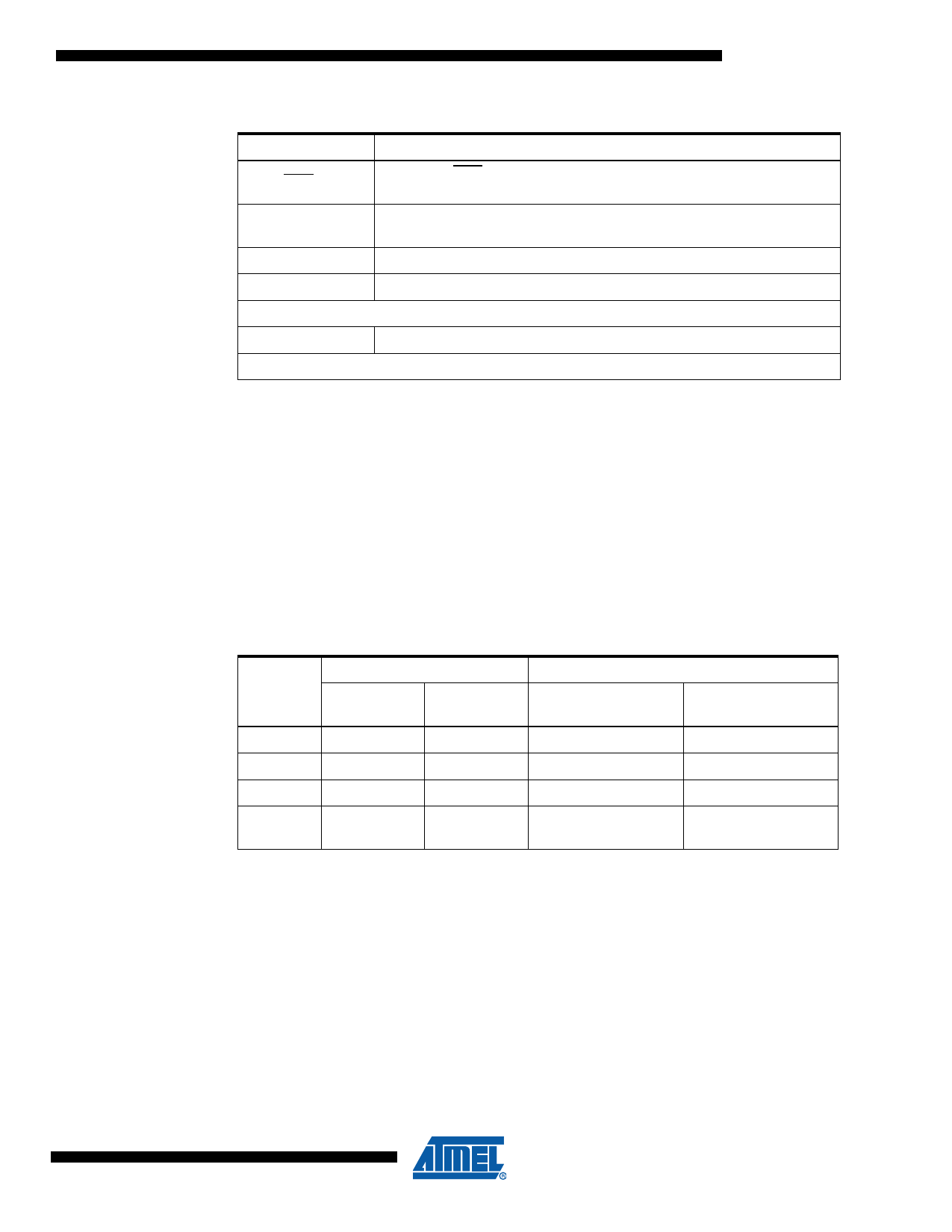
Table 2-3. Read Status Register Bit Definition
Bit
Definition
Bit 0 (RDY)
Bit 0 = “0” (RDY) indicates the device is ready. Bit 0 = “1” indicates the
write cycle is in progress.
Bit 1 (WEN)
Bit 1 = “0” indicates the device is not write enabled. Bit 1 = “1” indicates
the device is write enabled.
Bit 2 (BP0)
See Table 2-4.
Bit 3 (BP1)
See Table 2-4.
Bits 4-6 are 0s when device is not in an internal write cycle.
Bit 7 (WPEN)
See Table 2-5 on page 10.
Bits 0-7 are 1s during an internal write cycle.
READ PRODUCT ID (RDID): The RDID instruction allows the user to read the manufacturer
and product ID of the device. The first byte after the instruction will be the manufacturer code
(1FH = ATMEL), followed by the device code, 60H.
WRITE STATUS REGISTER (WRSR): The WRSR instruction allows the user to select one of
four levels of protection for the AT25F1024A. The AT25F1024A is divided into four sectors
where the top quarter (1/4), top half (1/2), or all of the memory sectors can be protected (locked
out) from write. Any of the locked-out sectors will therefore be Read only. The locked-out sector
and the corresponding status register control bits are shown in Table 2-4.
The three bits, BP0, BP1, and WPEN, are nonvolatile cells that have the same properties and
functions as the regular memory cells (e.g., WREN, tWC, RDSR).
Table 2-4. Block Write Protect Bits
Status Register Bits
AT25F1024A
Level
BP1
Array Addresses
Locked-out
BP0
Locked Out
Sector(s)
0
0
0
None
None
1(1/4)
0
1
018000 – 01FFFF
Sector 4
2(1/2)
1
0
010000 – 01FFFF
Sector 3, 4
3(All)
1
1
000000 – 01FFFF
All sectors
(1 – 4)
9
3346G–SFLSH–7/07
Share Link: 