AT49F1604 查看數據表(PDF) - Atmel Corporation
零件编号
产品描述 (功能)
生产厂家
AT49F1604 Datasheet PDF : 18 Pages
| |||
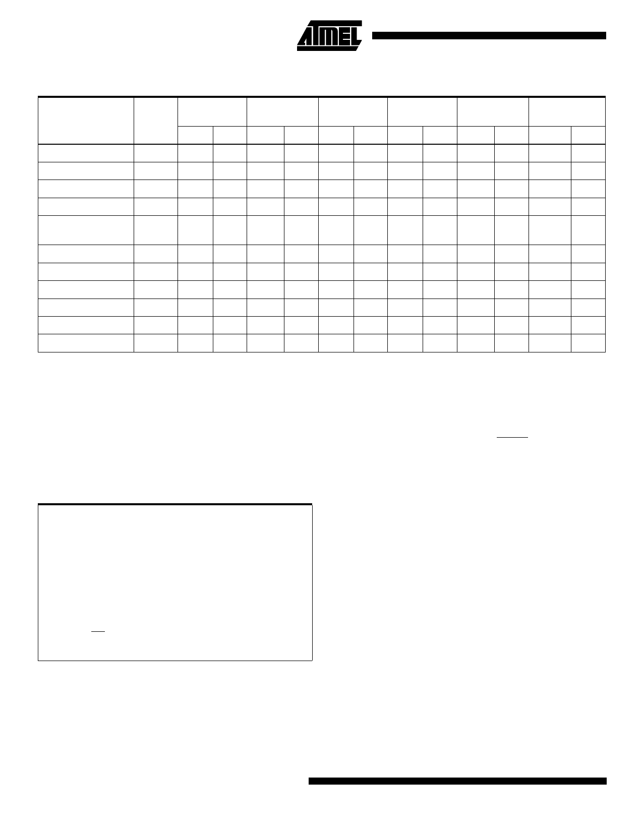
Command Definition in Hex(1)
Command
Sequence
Bus
Cycles
1st Bus
Cycle
Addr Data
2nd Bus
Cycle
Addr Data
3rd Bus
Cycle
Addr Data
4th Bus
Cycle
Addr Data
5th Bus
Cycle
Addr Data
6th Bus
Cycle
Addr Data
Read
Sector Erase
1
Addr DOUT
6
5555 AA 2AAA 55 5555 80 5555 AA 2AAA 55 SA(3)(4) 30
Byte/Word Program
4
5555 AA 2AAA 55 5555 A0 Addr DIN
Bypass Unlock
6
5555 AA 2AAA 55 5555 80 5555 AA 2AAA 55 5555 A0
Single Pulse
Byte/Word Program
1
Addr DIN
Sector Lockout
6
5555 AA 2AAA 55 5555 80 5555 AA 2AAA 55 SA(3)(4) 40
Erase Suspend
Erase Resume
1
xxxx B0
1
PA(5)
30
Product ID Entry
Product ID Exit(2)
Product ID Exit(2)
3
5555 AA 2AAA 55 5555 90
3
5555 AA 2AAA 55 5555 F0
1
xxxx F0
Notes:
1. The DATA FORMAT in each bus cycle is as follows: I/O15 - I/O8 (Don’t Care); I/O7 - I/O0 (Hex).
The ADDRESS FORMAT in each bus cycle is as follows: A15 - A0 (Hex). Address A19 through A14 are don’t care in the
word mode. Address A19 through A14 and A-1 are don’t care in the byte mode.
2. Either one of the Product ID Exit commands can be used.
3. SA = sector address. Any byte/word address within a sector can be used to designate the sector address (see next two
pages for details).
4. When the sector programming lockout feature is not enabled, the sector will erase (from the same Sector Erase command).
Once the sector has been protected, data in the protected sectors cannot be changed unless the RESET pin is taken to
12V ± 0.5V.
5. PA is the plane address (A19 - A18).
Absolute Maximum Ratings*
Temperature under Bias ................................ -55°C to +125°C
Storage Temperature ..................................... -65°C to +150°C
All Input Voltages
(including NC Pins)
with Respect to Ground ...................................-0.6V to +6.25V
All Output Voltages
with Respect to Ground .............................-0.6V to VCC + 0.6V
Voltage on OE
with Respect to Ground ...................................-0.6V to +13.5V
*NOTICE:
Stresses beyond those listed under “Absolute
Maximum Ratings” may cause permanent dam-
age to the device. This is a stress rating only and
functional operation of the device at these or any
other conditions beyond those indicated in the
operational sections of this specification is not
implied. Exposure to absolute maximum rating
conditions for extended periods may affect device
reliability.
6
AT49F1604(T)/1614(T)
Share Link: 