ATTINY40 查看數據表(PDF) - Atmel Corporation
零件编号
产品描述 (功能)
生产厂家
ATTINY40 Datasheet PDF : 216 Pages
| |||
ATtiny40
4. CPU Core
This section discusses the AVR core architecture in general. The main function of the CPU core
is to ensure correct program execution. The CPU must therefore be able to access memories,
perform calculations, control peripherals, and handle interrupts.
4.1 Architectural Overview
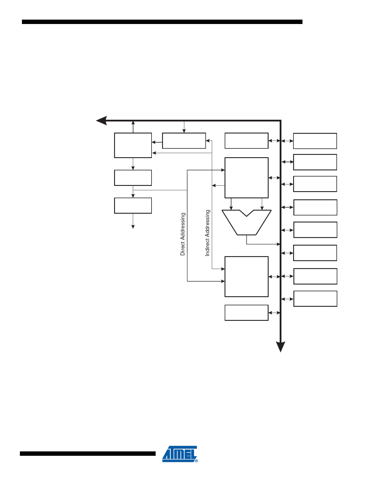
Figure 4-1. Block Diagram of the AVR Architecture
Data Bus 8-bit
Flash
Program
Memory
Instruction
Register
Instruction
Decoder
Control Lines
Program
Counter
Status
and Control
16 x 8
General
Purpose
Registrers
ALU
Interrupt
Unit
Watchdog
Timer
Analog
Comparator
ADC
Timer/Counter 0
Timer/Counter 1
Data
SRAM
I/O Lines
SPI
TWI Slave
8263A–AVR–08/10
In order to maximize performance and parallelism, the AVR uses a Harvard architecture – with
separate memories and buses for program and data. Instructions in the program memory are
executed with a single level pipelining. While one instruction is being executed, the next instruc-
tion is pre-fetched from the program memory. This concept enables instructions to be executed
in every clock cycle. The program memory is In-System Reprogrammable Flash memory.
The fast-access Register File contains 16 x 8-bit general purpose working registers with a single
clock cycle access time. This allows single-cycle Arithmetic Logic Unit (ALU) operation. In a typ-
ical ALU operation, two operands are output from the Register File, the operation is executed,
and the result is stored back in the Register File – in one clock cycle.
7
Share Link: 