AU5780 查看數據表(PDF) - Philips Electronics
零件编号
产品描述 (功能)
生产厂家
AU5780 Datasheet PDF : 10 Pages
| |||
Philips Semiconductors
SAE/J1850/VPW transceiver
Product specification
AU5780
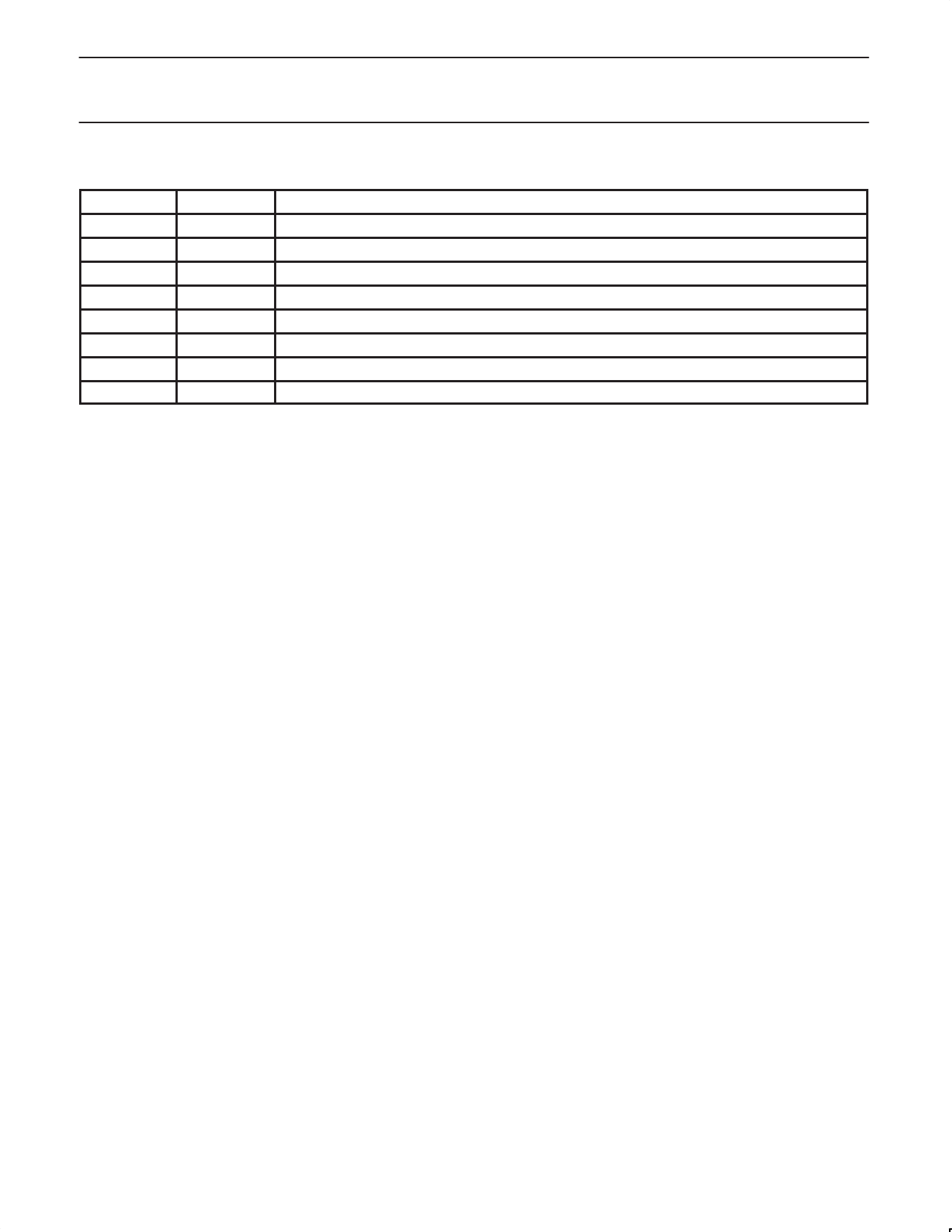
PIN DESCRIPTION
SYMBOL
PIN
BATT
1
TX
2
R/F
3
RX
4
BUS_IN
5
/LB
6
BUS_OUT
7
GND
8
DESCRIPTION
Battery supply input (12V nom.)
Transmit data input; low: transmitter passive; high: transmitter active
Rise/fall slew rate set input
Receive data output; low: active bus condition detected; float/high: passive bus condition detected
Bus line receive input
Loop-back test mode control input; low: loop-back mode; high: normal communication mode
Bus line transmit output
Ground
FUNCTIONAL DESCRIPTION
The AU5780 is an integrated line transceiver IC that interfaces an
SAE/J1850 protocol controller IC to the vehicle’s multiplexed bus
line. It is primarily intended for automotive “Class B” multiplexing
applications in passenger cars using VPW (Variable Pulse Width)
modulated signals with a nominal bit rate of 10.4 kbps. The AU5780
also receives messages in the so-called 4X mode where data is
transmitted with a typical bit rate of 41.6 kbps. The device provides
transmit and receive capability as well as protection to a J1850
electronic module.
A J1850 link controller feeds the transmit data stream to the
transceiver’s TX input. The AU5780 transceiver waveshapes the TX
data input signal with controlled rise & fall slew rates and rounded
shape. The bus output signal is transmitted with both voltage and
current control. The BUS_IN input is connected to the physical bus
line via an external resistor. The external resistor and an internal
capacitance provides filtering against RF bus noise. The incoming
signal is output at the RX pin being connected to the J1850 link
controller.
If the TX input is idle for a certain time, then the AU5780 enters a
low-power mode. This mode is dedicated to help meet ignition-off
current draw requirements. The BUS_IN input comparator is kept
alive in the low-power mode. Normal power mode will be entered
again upon detection of activity, i.e., rising edge at the TX input. The
device is able to receive and transmit a valid J1850 message when
initially in low-power mode.
The AU5780 features special robustness at its BATT and BUS_OUT
pins hence the device is well suited for applications in the
automotive environment. Specifically, the BATT input is protected
against 50V load dump, jump start and reverse battery condition.
The BUS_OUT output is protected against wiring fault conditions,
e.g., short circuit to battery voltage as well as typical automotive
transients (i.e., –200V / +200V). In addition, an overtemperature
shutdown function with hysteresis is incorporated which protects the
device under system fault conditions. The chip temperature is
sensed at the bus drive transistor in the output buffer. In case of the
chip temperature reaching the trip point, the AU5780 will latch-off
the transceiver function. The device is reset on the first rising edge
on the TX input after a small decrease of the chip temperature.
The AU5780 also provides a loop-back mode for diagnostic
purpose. If the /LB pin is open circuit or pulled low, then TX signal is
internally looped back to the RX output independent of the signals
on the bus. In this mode the electronic module is disconnected from
the bus, i.e., the TX signal is not output to the physical bus line. In
this mode, it can be used, e.g., for self-test purpose.
1998 Jun 30
4
Share Link: 