AZ100LVEL16VTXP 查看數據表(PDF) - Arizona Microtek, Inc
零件编号
产品描述 (功能)
生产厂家
AZ100LVEL16VTXP Datasheet PDF : 13 Pages
| |||
AZ100LVEL16VT
100K PECL DC Characteristics (VEE = GND, VCC = +5.0V)
Symbol
Characteristic
-40°C
Min
Max
0°C
Min
Max
25°C
Min
Max
VOH
Output HIGH Voltage1,3
3955
4165
4005
4165
4005
4165
VOH
Output HIGH Voltage1,5
3915
4120
3975
4120
3975
4120
VOL
Output LOW Voltage1,3,5
3075
3445
3100
3338
3100
3338
Input HIGH Voltage
VIH
D/D¯ , EN/E¯N¯ (PECL)1 3835
4120
3835
4120
3835
4120
EN (CMOS/TTL) 2000
VCC
2000
VCC
2000
VCC
Input LOW Voltage
VIL
D/D¯ , EN/E¯N¯ (PECL)1 3190
3525
3190
3525
3190
3525
EN (CMOS/TTL) GND
800
GND
800
GND
800
VBB
Reference Voltage1
3610
3750
3610
3750
3610
3750
IIL
Input LOW Current EN4
0.5
0.5
0.5
IIH
Input HIGH Current EN4
150
150
150
IEE
Power Supply Current2
48
48
48
1. For supply voltages other that 5.0V, use the ECL table values and ADD supply voltage value.
2. Specified with VEEP and CS-SEL open for VTL and VTX. Subtract 4mA for VTNA, VTNB, VTNC & VTND.
3. Specified with VEEP and CS-SEL connected to VEE for VTL and VTX only.
4. Specified with EN-SEL open for VTL and VTX only.
5. Specified with QHG/Q¯ HG connected with 50 Ω to VCC –2V for VTNA, VTNB, VTNC & VTND.
85°C
Unit
Min
Max
4005
4165
mV
3975
4120
mV
3100
3338
mV
3835
2000
4120
mV
VCC
3190
3525
mV
GND
800
3610
3750
mV
0.5
μA
150
μA
54
mA
AC Characteristics (VEE = -3.0V to -5.5V; VCC = GND or VEE = GND; VCC = +3.0V to +5.5V)
Symbol
Characteristic
-40°C
0°C
25°C
85°C
Unit
Min Typ Max Min Typ Max Min Typ Max Min Typ Max
tPLH / tPHL
Propagation Delay
D to Q/Q¯ Outputs1
(SE)
400
400
400
430 ps
D to QHG/Q¯ HG Outputs1 (SE)
550
550
550
630
tSKEW
Duty Cycle Skew2 (SE)
5
20
5
20
5
20
5
20 ps
VPP
Minimum Input Swing3 DIFF 80
SE
160
80
160
80
160
80
160
mV
tr / tf
Output Rise/Fall Times1
(20% - 80%)
100
260 100
260 100
260 100
260 ps
1. For VTL and VTX, output specified with VEEP and CS-SEL connected to VEE with an AC coupled 50Ω load. For VTNA, VTNB, VTNC &
VTND, AC coupled 50Ω on Q¯ to VCC –2V and DC coupled 50Ω to VCC –2V on QHG/Q¯ HG.
2. Duty cycle skew is the difference between a tPLH and tPHL propagation delay through a device.
3. VPP is the minimum peak-to-peak input swing for which AC parameters guaranteed. The device has a voltage gain of ≈ 20 to Q/Q¯ outputs and a
voltage gain of ≈ 100 to QHG/Q¯ HG outputs.
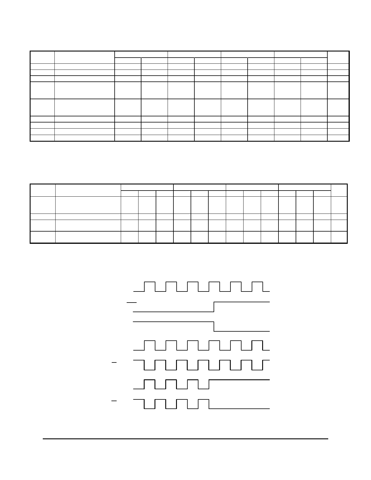
D
EN (VTL, VTX); EN (VTNA, VTNB)
(PECL)
EN (VTL, VTX, VTNC, VTND)
(CMOS)
Q
Q
QHG
QHG
TIMING DIAGRAM
April 2007 * REV - 9
www.azmicrotek.com
4
Share Link: 