MC100E336FN 查看數據表(PDF) - Motorola => Freescale
零件编号
产品描述 (功能)
生产厂家
MC100E336FN Datasheet PDF : 4 Pages
| |||
MOTOROLA
SEMICONDUCTOR TECHNICAL DATA
3ĆBit Registered Bus Transceiver
The MC10E/MC100E336 contains three bus transceivers with both
transmit and receive registers. The bus outputs (BUS0–BUS2) are
specified for driving a 25Ω bus; the receive outputs (Q0 – Q2) are
specified for 50Ω. The bus outputs feature a normal HIGH level (VOH) and
a cutoff LOW level — when LOW, the outputs go to –2.0V and the output
emitter-follower is “off”, presenting a high impedance to the bus. The bus
outputs also feature edge slow-down capacitors.
• 25Ω Cutoff Bus Outputs
• 50Ω Receiver Outputs
MC10E336
MC100E336
3-BIT REGISTERED
BUS TRANSCEIVER
• Transmit and Receive Registers
• 1500ps Max. Clock to Bus
• 1000ps Max. Clock to Q
• Bus Outputs Feature Internal Edge Slow-Down Capacitors
• Additional Package Ground Pins
• Extended 100E VEE Range of – 4.2V to – 5.46V
• 75kΩ Input Pulldown Resistors
The Transmit Enable pins (TEN) control whether current data is held in
the transmit register, or new data is loaded from the A/B inputs. A LOW on
both of the Bus Enable inputs (BUSEN), when clocked through the
register, disables the bus outputs to –2.0V.
The receiver section clocks bus data into the receive registers, after
gating with the Receive Enable (RXEN) input.
FN SUFFIX
PLASTIC PACKAGE
CASE 776-02
All registers are clocked by a positive transition of CLK1 or CLK2 (or
both).
Additional leadframe grounding is provided through the Ground pins (GND) which should be connected to 0V. The GND pins
are not electrically connected to the chip.
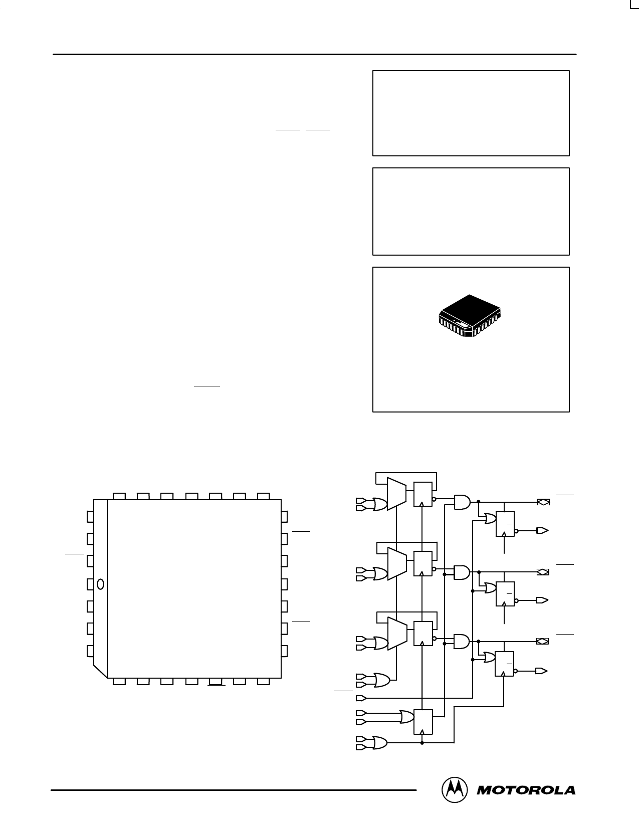
Pinout: 28-Lead PLCC (Top View)
LOGIC DIAGRAM
TEN2 TEN1 B2 A2 NC VCCO Q2
A0
25 24 23 22 21 20 19
B0
BUSEN1 26
18 GND
BUSEN2 27
17 BUS2
0 DQ
1
25 Ω CUTOFF
BUS0
D
Q
50 Ω Q0
RXEN 28
VEE 1
CLK1 2
16 VCC
A1
15 Q1
B1
14 VCCO
0 DQ
1
25 Ω CUTOFF
BUS1
D
50 Ω
Q
Q1
CLK2 3
13 BUS1
A0 4
12 GND
5 6 7 8 9 10 11
B0 A1 B1 VCCO BUS0 GND Q0
* All VCC and VCCO pins are tied together on the die.
A2
B2
TEN1
TEN2
RXEN
BUSEN1
BUSEN2
0
DQ
1
DQ
25 Ω CUTOFF
BUS2
D
50 Ω
Q
Q2
CLK1
CLK2
12/93
© Motorola, Inc. 1996
2–1
REV 2
Share Link: 