M52733SP 查看數據表(PDF) - MITSUBISHI ELECTRIC
零件编号
产品描述 (功能)
生产厂家
M52733SP Datasheet PDF : 12 Pages
| |||
MITSUBISHI ICs (Monitor)
M52733SP
3-CHANNEL VIDEO AMPLIFICATION WITH OSD BLANKING
3. Supposing that the measured value is treated as amplitude VOR1
(VOG1 or VOB1) when SG1 is input, as VOR8 (VOG8 or VOB8) when
SG2 is input, or as VOR9 (VOG9 or VOB9) when SG3 is input,
frequency characteristics FC1 and FC1' are calculated as follows:
VOR8 (VOG8, VOB8)
FC1=20LOG
VOR1 (VOG1, VOB1)
[VP-P]
[VP-P]
FC1'=20LOG VOR9 (VOG9, VOB9)
VOR1 (VOG1, VOB1)
[VP-P]
[VP-P]
4. Frequency relative band widths ∆FC1 and ∆FC1' are equal to the
difference in FC1 and FC1', respectively, between the channels.
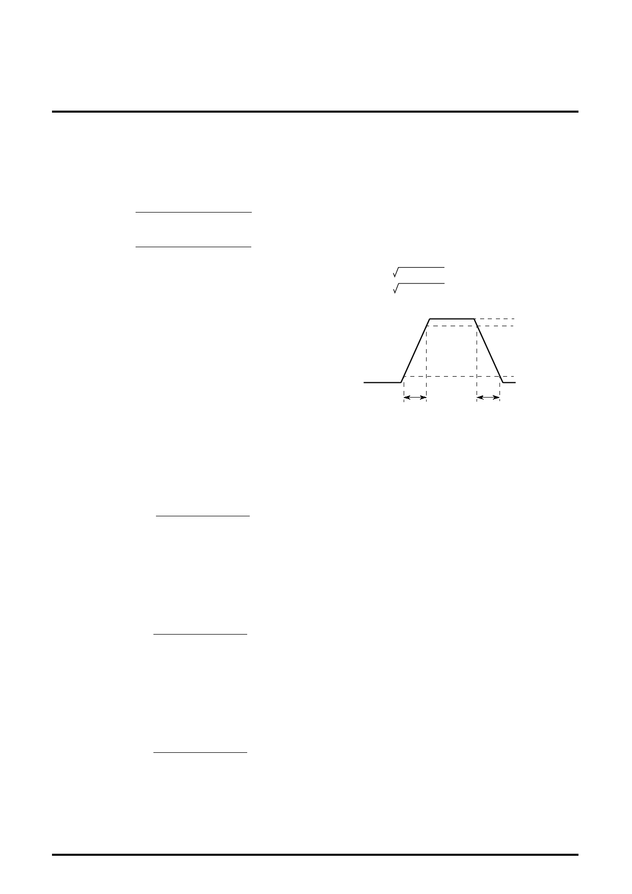
Tr Pulse characteristics1
Tf Pulse characteristics2
1. Measuring conditions are as given in Supplementary Table.
2. Measure the time needed for the input pulse to rise from 10% to
90% (Tr1) and to fall from 90% to 10% (Tf1) with an active prove.
3. Measure the time needed for the output pulse to rise from 10%
to 90% (Tr2) and to fall from 90% to 10% (Tf2) with an active
prove.
4. Pulse characteristics Tr and Tf are calculated by the equation
below:
Tr (nsec)= (Tr2)2-(Tr1)2
Tf (nsec)= (Tf2)2-(Tf1)2
FC2 Frequency characteristics2 (f=130MHz; maximum)
∆FC2' Frequency relative characteristics2
(f=130MHz; maximum)
Measuring conditions and procedure are the same as described in
FC1, ∆FC1, FC1', ∆FC1', except that CONTRAST (V14) is turned
down to 1.5V.
C.T.1 Crosstalk1 (f=50MHz)
C.T.1' Crosstalk1 (f=130MHz)
1. Measuring conditions are as given in Supplementary Table.
2. Input SG2 (or SG3) to pin 11 (R-ch) only, and then measure the
waveform amplitude output at T.P21 (25 or 29). The measured
value is called VOR, VOG and or VOB respectively.
3. Crosstalk C.T. 1 is calculated by the equation below:
VOG or VOB
C.T.1 =20LOG
(C.T.1')
VOR
[VP-P]
[dB]
[VP-P]
C.T.2 Crosstalk2 (f=50MHz)
C.T.2' Crosstalk2 (f=130MHz)
1. Change the input pin from pin 11 (R-ch) to pin 7 (G-ch), and
measure the output in the same way as in C.T.1, C.T.1'.
2. Crosstalk C.T. 2 is calculated by the equation below:
VOR or VOB
C.T.2 =20LOG
(C.T.2')
VOG
[VP-P]
[dB]
[VP-P]
C.T.3 Crosstalk3 (f=50MHz)
C.T.3' Crosstalk3 (f=130MHz)
1. Change the input pin from pin 11 (R-ch) to pin 3 (B-ch), and
measure the output in the same way as in C.T.1, C.T.1'.
2. Crosstalk C.T. 3 is calculated by the equation below:
VOR or VOG
C.T.3 =20LOG
(C.T.3')
VOB
[VP-P]
[dB]
[VP-P]
100%
90%
10%
0%
Tr
Tf
V14th Clamp pulse threshold voltage
1. Measuring conditions are as given in Supplementary Table.
2. Turn down the SG5 input level gradually, monitoring the output
(about 2.0 VDC). Measure the SG5 input level when the output
reaches 0V.
W14 Clamp pulse minimum width
Under the same conditions as given in V14th, reduce the SG5 pulse
width gradually, monitoring the output. Measure the SG5 pulse
width when the output reaches 0V.
PDCH Pedestal voltage temperatere characteristics1
PDCL Pedestal voltage temperatere characteristics2
1. Measuring conditions are as given in Supplementary Table.
2. Measure the pedestal voltage at room temperature.
The measured value is called PDC1.
3. Measure the pedestal voltage at temperatures of -20°C and
85°C. The measured value is called, respectively, PDC2 and
PDC3.
4. PDCH=PDC1 - PDC2
PDCL=PDC1 - PDC3
V1th BLK input threshold voltage
1. Measuring conditions are as given in Supplementary Table.
2. Make sure that signals are not being output synchronously with
SG7 (blanking period).
3. Reduce the SG7 input level gradually, monitoring output.
Measure the SG7 level when the blanking period disappears.
The measured value is called V1th.
6
Share Link: 