AZ100LVE111EFNR2 查看數據表(PDF) - AZ Microtek
零件编号
产品描述 (功能)
生产厂家
AZ100LVE111EFNR2 Datasheet PDF : 6 Pages
| |||
AZ10LVE111E
AZ100LVE111E
100K PECL DC Characteristics (VEE = GND, VCC = VCCO = +5.0V)
Symbol
Characteristic
-40°C
0°C
25°C
85°C
Unit
Min Typ Max Min Typ Max Min Typ Max Min Typ Max
VOH
Output HIGH Voltage1,2 3915 3995 4120 3975 4045 4120 3975 4045 4120 3975 4045 4120 mV
VOL
Output LOW Voltage1,2
3170 3305 3445 3190 3295 3380 3190 3295 3380 3190 3295 3380
mV
VIH
Input HIGH Voltage1
3835
4120 3835
4120 3835
4120 3835
4120 mV
VIL
Input LOW Voltage1
3190
3525 3190
3525 3190
3525 3190
3525 mV
VBB
Reference Voltage1
3620
3740 3620
3740 3620
3740 3620
3740 mV
IIH
Input HIGH Current
150
150
150
150
μA
IIL
Input LOW Current
0.5
0.5
0.5
0.5
μA
IEE
Power Supply Current
48
60
48
60
48
60
55
69
mA
1. For supply voltages other that 5.0V, use the ECL table values and ADD supply voltage value.
2. Each output is terminated through a 50Ω resistor to VCC – 2V.
AC Characteristics (VEE = -3.0V to -5.5V, VCC = VCCO = GND or VEE = GND, VCC = VCCO = +3.0 to +5.5V)
Symbol
Characteristic
-40°C
0°C
25°C
85°C
Unit
Min Typ Max Min Typ Max Min Typ Max Min Typ Max
Propagation Delay
tPLH / tPHL to Output
IN (Diff)1 380
IN (SE)2 280
Enable3 400
Disable3 400
650 460
700 410
900 450
900 450
560 480
610 430
850 450
850 450
580 510
630 460
850 450
850 450
610
660 ps
850
850
tS
Setup Time E¯N¯ to IN5 250
0
200
0
200
0
200
0
ps
tH
Hold Time IN to E¯N¯ 6 50 -200
0
-200
0
-200
0
-200
ps
tR
Release Time E¯N¯ to IN7 350
100
300 100
300 100
300 100
ps
tskew
Within-Device Skew4
25
75
25
50
25
50
25
50
ps
VPP (AC) Minimum Input Swing8 250
250
250
250
mV
VCMR
Common Mode Range9
VEE +
1.8
VCC -
0.4
VEE +
1.8
VCC -
0.4
VEE +
1.8
VCC -
0.4
VEE +
1.8
VCC -
0.4
V
tr / tf
Rise/Fall Time
250
650 275
600 275
600 275
600 ps
1. The differential propagation delay is defined as the delay from the crossing point of the differential input signals to the crossing point of the
differential output signals.
2. The single-ended propagation delay is defined as the delay from the 50% point of the input signal to the 50% point of the output signal.
3. Enable is defined as the propagation delay from the 50% point of a negative transition on E¯N¯ to the 50% point of a positive transition on Q (or a
negative transition on Q¯ ). Disable is defined as the propagation delay from the 50% point of a positive transition on E¯N¯ to the 50% point of a
negative transition on Q (or a positive transition on Q¯ ).
4. The within-device skew is defined as the worst-case difference between any two similar delay paths within a single device.
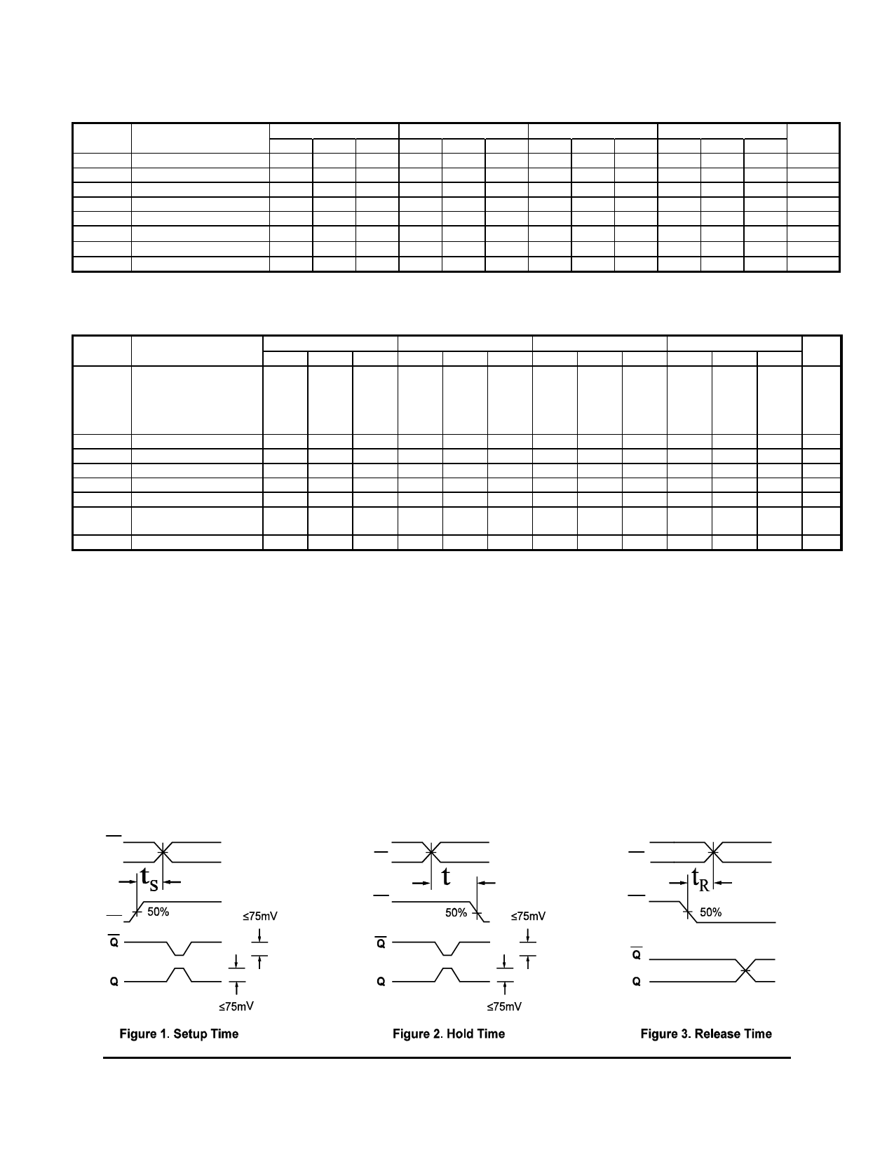
5. The setup time is the minimum time that E¯N¯ must be asserted prior to the next transition of IN/I¯N¯ to prevent an output response greater than
±75mV to that IN/I¯N¯ transition (see Figure 1).
6. The hold time is the minimum time that E¯N¯ must remain asserted after a negative going IN or a positive going I¯N¯ to prevent an output response
greater than ±75 mV to that IN/I¯N¯ transition (see Figure 2).
7. The release time is the minimum time that E¯N¯ must be de-asserted prior to the next IN/I¯N¯ transition to ensure an output response that meets the
specified IN to Q propagation delay and output transition times (see Figure 3).
8. VPP is defined as the minimum peak-to-peak differential input swing for which AC parameters are guaranteed. The VPP(min) is AC limited for the
LVE111E, because differential input as low as 50 mV will still produce full ECL levels at the output.
9. VCMR is defined as the range within which the VIH level may vary, with the device still meeting the propagation delay specification. The VIL level
must be such that the peak-to-peak voltage is less than 1.0 V and greater than or equal to VPP(min).
IN
IN
IN
IN
IN
IN
H
EN
EN
EN
November 2006 * REV - 4
www.azmicrotek.com
4
Share Link: 