AZM100LVE310R2 查看數據表(PDF) - AZ Microtek
零件编号
产品描述 (功能)
生产厂家
AZM100LVE310R2 Datasheet PDF : 5 Pages
| |||
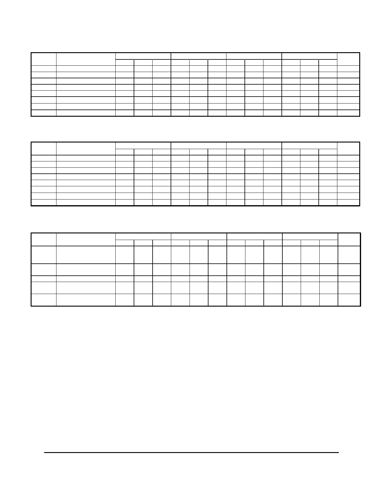
AZ100LVE310
100K LVPECL DC Characteristics (VEE = GND, VCC = VCCO = +3.3V)
Symbol
Characteristic
-40°C
0°C
25°C
85°C
Unit
Min Typ Max Min Typ Max Min Typ Max Min Typ Max
VOH
Output HIGH Voltage1,2 2215 2295 2420 2275 2345 2420 2275 2345 2420 2275 2345 2420 mV
VOL
Output LOW Voltage1,2
1470 1605 1745 1490 1595 1680 1490 1595 1680 1490 1595 1680
mV
VIH
Input HIGH Voltage1
2135
2420 2135
2420 2135
2420 2135
2420 mV
VIL
Input LOW Voltage1
1490
1825 1490
1825 1490
1825 1490
1825 mV
VBB
Reference Voltage1
1920
2040 1920
2040 1920
2040 1920
2040 mV
IIH
Input HIGH Current
150
150
150
150
μA
IIL
Input LOW Current
0.5
0.5
0.5
0.5
μA
IEE
Power Supply Current
55
60
55
60
55
60
65
70
mA
1. For supply voltages other that 3.3V, use the ECL table values and ADD supply voltage value.
2. Each output is terminated through a 50Ω resistor to VCC – 2V.
100K PECL DC Characteristics (VEE = GND, VCC = VCCO = +5.0V)
Symbol
Characteristic
-40°C
0°C
25°C
85°C
Unit
Min Typ Max Min Typ Max Min Typ Max Min Typ Max
VOH
Output HIGH Voltage1,2 3915 3995 4120 3975 4045 4120 3975 4045 4120 3975 4045 4120 mV
VOL
Output LOW Voltage1,2
3170 3305 3445 3190 3295 3380 3190 3295 3380 3190 3295 3380
mV
VIH
Input HIGH Voltage1
3835
4120 3835
4120 3835
4120 3835
4120 mV
VIL
Input LOW Voltage1
3190
3525 3190
3525 3190
3525 3190
3525 mV
VBB
Reference Voltage1
3620
3740 3620
3740 3620
3740 3620
3740 mV
IIH
Input HIGH Current
150
150
150
150
μA
IIL
Input LOW Current
0.5
0.5
0.5
0.5
μA
IEE
Power Supply Current
55
60
55
60
55
60
65
70
mA
1. For supply voltages other that 5.0V, use the ECL table values and ADD supply voltage value.
2. Each output is terminated through a 50Ω resistor to VCC – 2V.
AC Characteristics (VEE = -3.0V to -5.5V, VCC = VCCO = GND or VEE = GND, VCC = VCCO = +3.0 to +5.5V)
Symbol
Characteristic
-40°C
0°C
25°C
85°C
Unit
Min Typ Max Min Typ Max Min Typ Max Min Typ Max
Propagation Delay to
tPLH / tPHL Output
IN (Diff)1 525
IN (SE)2 500
725 550
750 550
750 550
775 550
750 575
800 600
775
ps
850
tSKEW
VPP (AC)
VCMR
Within-Device Skew
Part-to-Part Skew (Diff)3
Minimum Input Swing4
Common Mode Range5
250
VEE +
1.8
75
250
VCC -
0.4
250
VEE +
1.8
75
250
VCC -
0.4
250
VEE +
1.8
50
200
VCC -
0.4
250
VEE +
1.8
50
ps
200
mV
VCC -
0.4
V
tr / tf
Rise/Fall Time
20 – 80%
250 450 650 275 375 600 275 375 600 275 375 600
ps
1. The differential propagation delay is defined as the delay from the crossing point of the differential input signals to the crossing point of the
differential output signals.
2. The single-ended propagation delay is defined as the delay from the 50% point of the input signal to the 50% point of the output signal.
3. The within-device skew is defined as the worst-case difference between any two similar delay paths within a single device.
4. VPP is the minimum peak-to-peak differential input swing for which AC parameters are guaranteed. The VPP(min) is AC limited for the LVE310,
because differential input as low as 50 mV will still produce full ECL levels at the output.
5. VCMR is defined as the range within which the VIH level may vary, with the device still meeting the propagation delay specification. The VIL level
must be such that the peak-to-peak voltage is less than 1.0V and greater than or equal to VPP(min).
November 2006 * REV - 4
www.azmicrotek.com
3
Share Link: 