BGE847BO/SC0 查看數據表(PDF) - Philips Electronics
零件编号
产品描述 (功能)
生产厂家
BGE847BO/SC0 Datasheet PDF : 12 Pages
| |||
Philips Semiconductors
Optical receiver modules
Product specification
BGE847BO; BGE847BO/FC0;
BGE847BO/SC0
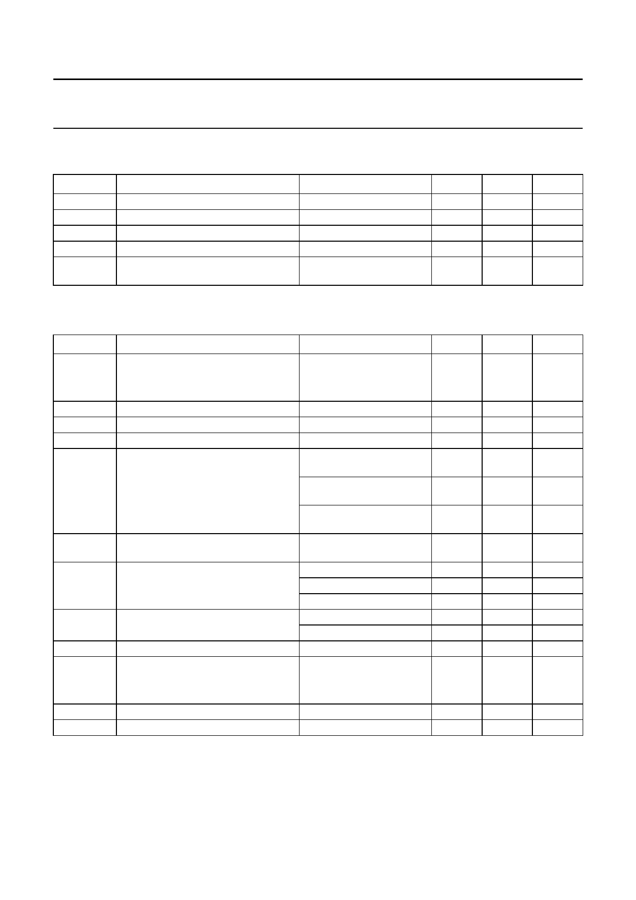
LIMITING VALUES
In accordance with the Absolute Maximum Rating System (IEC 60134).
SYMBOL
f
Tstg
Tmb
Pin
ESD
PARAMETER
frequency range
storage temperature
operating mounting base temperature
optical input power
ESD sensitivity
CONDITIONS
continuous
human body model;
R = 1.5 kΩ; C = 100 pF
MIN.
40
−40
−20
−
500
MAX.
870
+85
+85
5
−
UNIT
MHz
°C
°C
mW
V
CHARACTERISTICS
Bandwidth 40 to 870 MHz; VB = 24 V; Tmb = 30 °C; ZS = ZL = 75 Ω.
SYMBOL
PARAMETER
CONDITIONS
S
responsivity
λ = 1300 nm
BGE847BO
BGE847BO/FC0, BGE847BO/SC0
FL
flatness straight line (peak to valley) f = 40 to 870 MHz
S22
output return losses
optical input return losses
f = 40 to 870 MHz
d2
second order distortion
fm = 446.5 MHz;
notes 1 and 3
fm = 746.5 MHz;
notes 1 and 4
fm = 854.5 MHz;
notes 1 and 5
d3
third order distortion
fm = 853.25 MHz;
notes 2 and 6
F
equivalent noise input
f = 40 to 450 MHz
f = 450 to 750 MHz
f = 750 to 870 MHz
sλ
spectral sensitivity
λ = 1310 ±20 nm
λ = 1550 ±20 nm
λ
optical wavelength
L
length of optical fibre
fibre; SM type; 9/125 µm
BGE847BO
BGE847BO/FC0, BGE847BO/SC0
Itot
total current consumption (DC)
Ipin 4
photo diode bias current (DC)
MIN.
MAX.
UNIT
800
750
−
11
45
−
−
−
−
−
0.85
0.9
1 290
−
−
1
−
−
−68
−63
−57
−75
7
9
10.5
−
−
1 600
V/W
V/W
dB
dB
dB
dB
dB
dB
dB
pA/√Hz
pA/√Hz
pA/√Hz
A/W
A/W
nm
1
−
m
746
861
mm
175
205
mA
−
25
mA
2000 Apr 04
3
Share Link: 