BP5310A 查看數據表(PDF) - ROHM Semiconductor
零件编号
产品描述 (功能)
生产厂家
BP5310A Datasheet PDF : 6 Pages
| |||
BP5310A
Electrical characteristics (unless otherwise noted, Ta=25°C, VCTL=5V)
Parameter
Symbol Min. Typ. Max. Unit
Conditions
Input voltage
VIN
4.75 5.00 5.25
V
Output current
IOUT
−
−
120
mA
Output voltage
VOUT
11.4 12.0 12.6
V
VIN=4.75∼5.25V
IOUT=0~120mA
Ripple noise voltage
υ1
−
100
200
mVPP VIN=5V, IOUT=60mA
∗1
Efficiency
η
65
73
−
%
VIN=5V, IOUT=60mA
ON/OFF CTL voltage when ON
VCTL
3.3
−
−
V
VIN=5V, VOUT≥11.4V
∗2
ON/OFF CTL voltage when OFF
VCTL
−
−
0.4
V
VIN=4.75∼5.25V
ON/OFF CTL sink current
when ON
ISINK
−
0.8
1.3
mA
VIN=5V
VCTL=3.3V
∗3
ON/OFF CTL source current
when OFF
ISOURCE
−
1.0
1.5
mA
VIN=5V
VCTL=0.4V
∗4
∗1 Measured with a band width of 20 MHz.
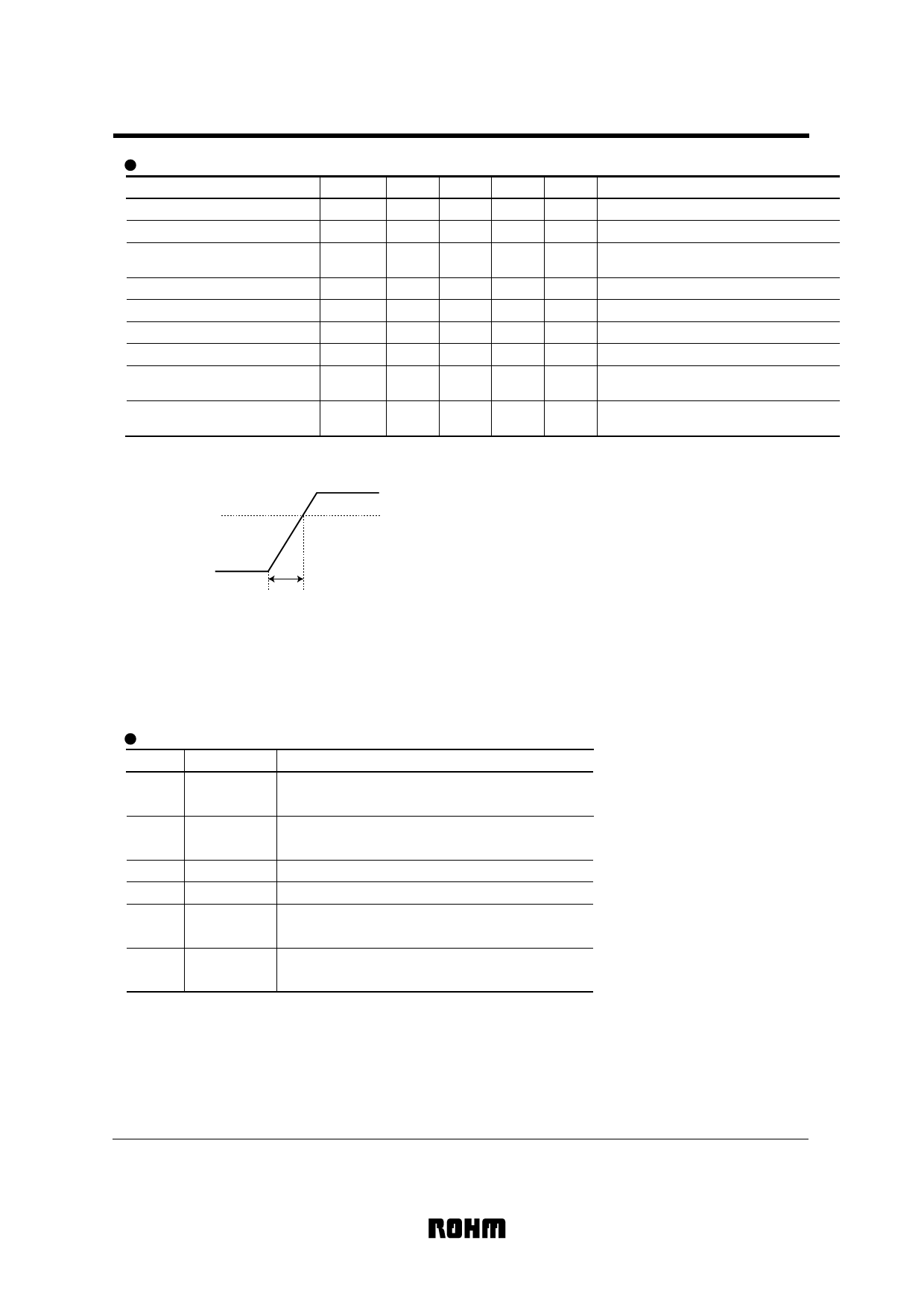
∗2 Ensure that the HIGH signal of the CTL pin(pin 8)rises in less than 100µS to the level at which the output turns on.
3.3V
0V
Less than 100µS
∗3 When the HIGH signal is applied to the CTL pin , a current flows into the CTL pin for a short period until the output rises. Little current flows thereafter.
∗4 When the LOW signal is applied to the CTL pin to turn OFF the output, a current flows from the CTL pin for a short period until the output drops to 0V.
Ensure that the control circuit can sink this current.
Pin descriptions
Pin No. Pin name
1
Co
2
VOUT
3
TP
4, 7
GND
8
VCTL
9
VIN
Function
Output smoothing capacitor connection pin; connect a
low-impedance capacitor with a recommended
capacitance of 47µF between this pin and GND
Output pin; connect an output capacitor with a
recommended capacitance of 2.2µF between this pin
and GND
Test pin; use this internally connected pin in OPEN mode
Ground pin
Output ON/OFF control pin; output starts when the pin is
HIGH level, and stops at LOW level
Input pin; connect a low-impedance capacitor with a
recommended capacitance of 100µF between this pin
and GND
2/5
Share Link: 