BR93LC46-W жҹҘзңӢж•ёж“ҡиЎЁпјҲPDFпјү - ROHM Semiconductor
йӣ¶д»¶зј–еҸ·
дә§е“ҒжҸҸиҝ° (еҠҹиғҪ)
з”ҹдә§еҺӮ家
BR93LC46-W Datasheet PDF : 11 Pages
| |||
Memory ICs
BR93LC46-W / BR93LC46F-W / BR93LC46RF-W /
BR93LC46FJ-W / BR93LC46RFJ-W / BR93LC46FV-W
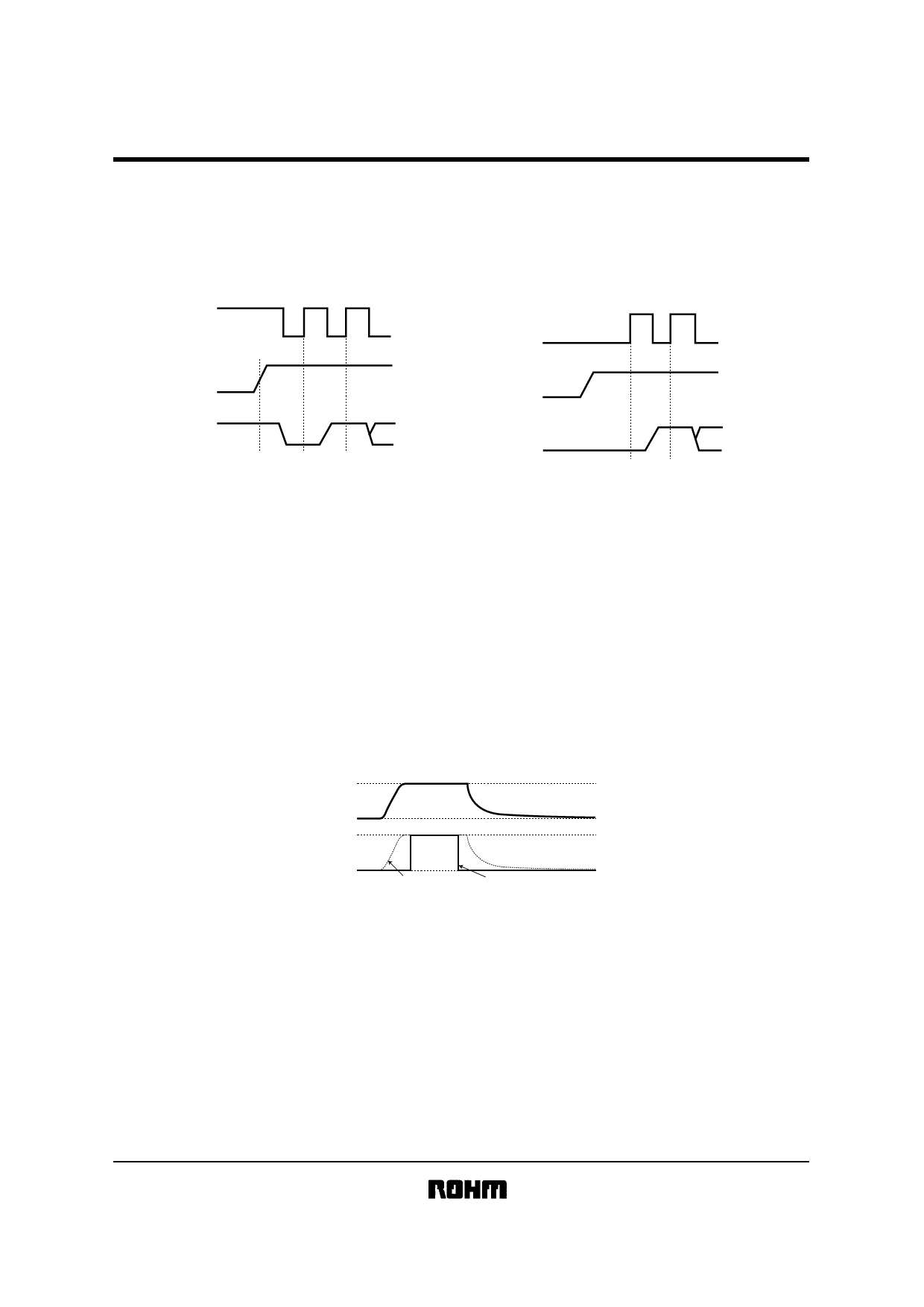
(2) Timing in the standby mode
As shown in Fig.16, during standby, if CS rises when SK is HIGH, the DI state may be read on the rising edge. If this
happens, and DI is HIGH, this is taken to be the start bit, causing a bit error (see point вҖңaвҖқ in Fig.16).
Make sure all inputs are LOW during standby or when turning the power supply on or off (see Fig.17).
Point a: Start bit position during erroneous operation
Point b: Timing during normal operation
SK
SK
CS
CS
DI
0
1
a
b
Fig. 16 Erroneous operation timing
DI
0
1
b
Fig. 17 Normal operation timing
(3) Precautions when turning power on and off
When turning the power supply on and off, make sure CS is set to LOW (see Fig.18).
When CS is HIGH, the EEPROM enters the active state. To avoid this, make sure CS is set to LOW (disable mode)
when turning on the power supply. (When CS is LOW, all input is cancelled.)
When the power supply is turned off, the low power state can continue for a long time because of the capacity of the
power supply line. Erroneous operations and erroneous writing can occur at such times for the same reasons as
described above. To avoid this, make sure CS is set to LOW before turning off the power supply.
To prevent erroneous writing, these ICs are equipped with a POR (Power On Reset) circuit, but in order to achieve
operation at a low power supply, VCC is set to operate at approximately 1.3V. After the POR has been activated,
writing is disabled, but if CS is set to HIGH, writing may be enabled because of noise or other factors. However, the
POR circuit is effective only when the power supply is on, and will not operate when the power is off.
Also, to prevent erroneous writing at low voltages, these ICs are equipped with a built-in circuit (VCC-lockout circuit)
which resets the write command if VCC drops to approximately 2V or lower (typ.) (вҲ—).
+ 5V
VCC
GND
+ 5V
CS
GND
Bad example
Good example
(Bad example)
(Good example)
Here, the CS pin is pulled up to VCC. In this case,
CS is HIGH (active state). Please be aware that the EEPROM may
perform erroneous operations or write erroneous data because of
noise or other factors. Please be aware that this can occur even if
the CS input is HIGH-Z.
In this case, CS is LOW when the power supply is turned
on or off.
Fig. 18
(4) Clock (SK) rise conditions
If the clock pin (SK) signal of the BR93LC46-W has a long rise time (tr) and if noise on the signal line exceeds a
certain level, erroneous operation can occur due to erroneous counts in the clock. To prevent this, a Schmitt trigger is
built into the SK input of the BR93LC46-W. The hysteresis amplitude of this circuit is set to approximately 0.2V, so if
the noise exceeds the SK input, the noise amplitude should be set to 0.2VP-P or lower. Furthermore, rises and falls in
the clock input should be accelerated as much as possible.
Share Link: 