BS616LV8017(2004) 查看數據表(PDF) - Brilliance Semiconductor
零件编号
产品描述 (功能)
生产厂家
BS616LV8017 Datasheet PDF : 9 Pages
| |||
BSI
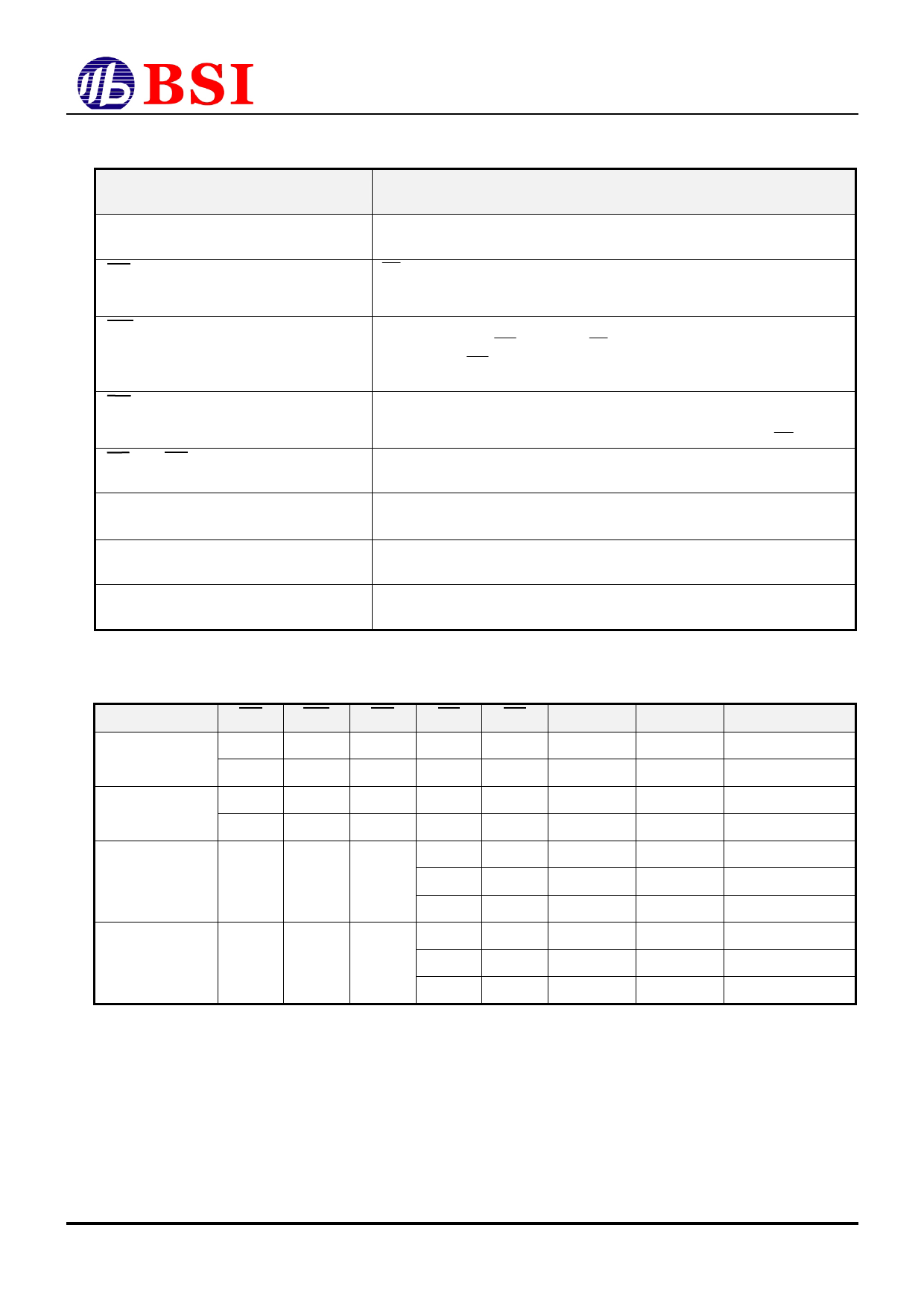
PIN DESCRIPTIONS
Name
A0-A18 Address Input
BS616LV8017
Function
These 19 address inputs select one of the 524,288 x 16-bit words in the RAM.
CE Chip Enable Input
CE is active LOW. Chip enables must be active when data read from or write to the
device. if chip enable is not active, the device is deselected and is in a standby power
mode. The DQ pins will be in the high impedance state when the device is deselected.
WE Write Enable Input
OE Output Enable Input
LB and UB Data Byte Control Input
The write enable input is active LOW and controls read and write operations. With the
chip selected, when WE is HIGH and OE is LOW, output data will be present on the
DQ pins; when WE is LOW, the data present on the DQ pins will be written into the
selected memory location.
The output enable input is active LOW. If the output enable is active while the chip is
selected and the write enable is inactive, data will be present on the DQ pins and they
will be enabled. The DQ pins will be in the high impedance state when OE is inactive.
Lower byte and upper byte data input/output control pins.
D0 - D15 Data Input/Output Ports These 16 bi-directional ports are used to read data from or write data into the RAM.
Vcc
Power Supply
Vss
Ground
TRUTH TABLE
MODE
CE WE OE
LB
UB
Not selected
H
X
X
X
X
(Power Down)
X
X
X
H
H
Output Disabled
L
X
X
H
H
L
H
H
X
X
L
L
Read
L
H
L
H
L
L
H
L
L
Write
L
L
X
H
L
L
H
ABSOLUTE MAXIMUM RATINGS(1)
SYMBOL
VTERM
TBIAS
PARAMETER
Terminal Voltage with
Respect to GND
Temperature Under Bias
RATING
-0.5 to
Vcc+0.5
-40 to +85
UNITS
V
OC
TSTG
Storage Temperature
-60 to +150
OC
D0~D7
D8~D15
Vcc CURRENT
High Z
High Z
I , I CCSB CCSB1
High Z
High Z
High Z
High Z
I , I CCSB CCSB1
ICC
High Z
High Z
ICC
Dout
Dout
ICC
High Z
Dout
ICC
Dout
High Z
ICC
Din
Din
ICC
X
Din
ICC
Din
X
ICC
OPERATING RANGE
RANGE
AMBIENT
TEMPERATURE
Vcc
Commercial 0O C to +70O C
2.4V ~ 5.5V
Industrial
-40O C to +85O C
2.4V ~ 5.5V
PT
Power Dissipation
1.0
W
CAPACITANCE (1) (TA = 25oC, f = 1.0 MHz)
IOUT
DC Output Current
20
mA
SYMBOL PARAMETER CONDITIONS MAX. UNIT
1. Stresses greater than those listed under ABSOLUTE MAXIMUM
RATINGS may cause permanent damage to the device. This is a
stress rating only and functional operation of the device at these
or any other conditions above those indicated in the operational
CIN
Input
VIN=0V
10
pF
Capacitance
CDQ
Input/Output
VI/O=0V
12
pF
Capacitance
sections of this specification is not implied. Exposure to absolute 1. This parameter is guaranteed and not 100% tested.
maximum rating conditions for extended periods may affect reliability.
R0201-BS616LV8017
2
Revision 2.1
Jan. 2004
Share Link: 