BU3072HFV-TR 查看數據表(PDF) - ROHM Semiconductor
零件编号
产品描述 (功能)
生产厂家
BU3072HFV-TR Datasheet PDF : 21 Pages
| |||
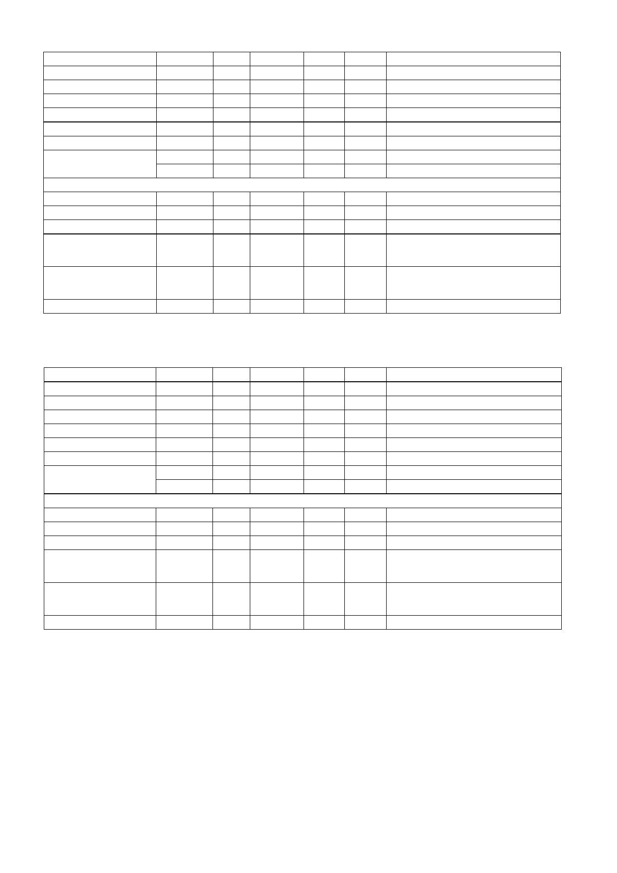
BU7322HFV(Ta=25℃, VDD=3.3V, Crystal frequency=27.0000MHz, unless otherwise specified.)
Parameter
Symbol Min.
Typ.
Max. Unit
Conditions
Output H voltage
VOH
2.8
-
-
V
IOH=-4.0mA
Output L voltage
VOL
-
-
0.5
V
IOL=4.0mA
Pull-down resistance
Rpd
25
50
100
kΩ Pull-down resistance on input pin
Consumption current 1
IDD
-
10
13.5
mA 49.5MHz output, at no load
Consumption current 2
IDD2
-
9.5
13.0
mA 36.0MHz output, at no load
Standby current
IDDst
-
-
1
μA OE=L
Output frequency
CLK_49.5
-
49.5000
-
MHz SEL=L, IN*66/6/6
CLK_36
-
36.0000
-
MHz SEL=H, IN*64/6/8
The following parameters represent design guaranteed performance.
Duty
Duty
45
50
55
% Measured at a voltage of 1/2 of VDD
Period-Jitter 1σ
PJsSD
-
50
-
psec ※1
Period-Jitter MIN-MAX PJsABS
-
300
Rise time
tr
-
2.5
Fall time
tf
-
2.5
-
psec ※2
Period of transition time required for the
-
nsec output to reach 80% from 20% of VDD.
Provided with 15pF output load.
Period of transition time required for the
-
nsec output to reach 20% from 80% of VDD.
Provided with 15pF output load.
Output Lock time
tLOCK
-
-
200
usec ※3
Note) The output frequency is determined by the arithmetic (frequency division) expression of a frequency input to IN.
If the input frequency is set to 27.0000MHz, the output frequency will be as listed above.
BU7325HFV(Ta=25℃, VDD=3.3V, Crystal frequency=27.0000MHz, unless otherwise specified.)
Parameter
Output H voltage
Output L voltage
Pull-down resistance
Consumption current 1
Consumption current 2
Standby current
Output frequency
Symbol
VOH
VOL
Rpd
IDD1
IDD2
IDDst
CLK_48
CLK_78
Min.
Typ.
Max.
2.8
-
-
-
-
0.5
25
50
100
-
11
15
-
12
16.5
-
-
1
-
48.0000
-
-
78.0000
-
Unit
V
V
kΩ
mA
mA
μA
MHz
MHz
Conditions
IOH=-4.0mA
IOL=4.0mA
Pull-down resistance on input pin
OE=H, SEL=L, at no load
OE=H, SEL=H, at no load
OE=L
SEL=L, IN*96/9/6
SEL=H, IN*104/9/4
The following parameters represent design guaranteed performance.
Duty
Duty
45
50
55
Period-Jitter 1σ
PJsSD
-
50
-
Period-Jitter MIN-MAX PJsABS
-
300
-
Rise time
tr
-
1.5
-
Fall time
tf
-
1.5
-
Output Lock time
tLOCK
-
-
200
%
psec
psec
nsec
nsec
usec
Measured at a voltage of 1/2 of VDD
※1
※2
Period of transition time required for the
output to reach 80% from 20% of VDD.
Provided with 15pF output load.
Period of transition time required for the
output to reach 20% from 80% of VDD.
Provided with 15pF output load.
※3
Note) The output frequency is determined by the arithmetic (frequency division) expression of a frequency input to IN.
If the input frequency is set to 27.0000MHz, the output frequency will be as listed above.
Common to BU3071HFV, BU3072HFV, BU3073HFV, BU3076HFV, BU7322HFV, BU7325HFV
1 Period-Jitter 1σ
This parameter represents standard deviation (1σ) on cycle distribution data at the time when the output clock cycles are
sampled 1000 times consecutively with the TDS7104 Digital Phosphor Oscilloscope of Tektronix Japan, Ltd.
2 Period-Jitter MIN-MAX
This parameter represents a maximum distribution width on cycle distribution data at the time when the output clock cycles are
sampled 1000 times consecutively with the TDS7104 Digital Phosphor Oscilloscope of Tektronix Japan, Ltd.
3 Output Lock Time
This parameter represents elapsed time after power supply turns ON to reach a voltage of 3.0 V, after the system is switched from
Power-Down state to normal operation state, or after the output frequency is switched, until it is stabilized at a specified frequency,
respectively.
4/20
Share Link: 