WED9LC6816V1310BC 查看數據表(PDF) - White Electronic Designs => Micro Semi
零件编号
产品描述 (功能)
生产厂家
WED9LC6816V1310BC Datasheet PDF : 27 Pages
| |||
White Electronic Designs
WED9LC6816V
256Kx32 SSRAM/4Mx32 SDRAM
EXTERNAL MEMORY SOLUTION FOR TEXAS INSTRUMENTS
TMS320C6000 DSP
DESCRIPTION
FEATURES
The WED9LC6816V is a 3.3V, 256K x 32 Synchronous
Clock speeds:
SSRAM: 200, 166,150, and 133 MHz
SDRAMs: 125 and 100 MHz
Pipeline SRAM and a 4Mx32 Synchronous DRAM array
constructed with one 256K x 32 SBSRAM and two 4Mx16
SDRAM die mounted on a multilayer laminate substrate.
The device is packaged in a 153 lead, 14mm x 22mm,
DSP Memory Solution
BGA.
Texas Instruments TMS320C6201
Texas Instruments TMS320C6701
Packaging:
The WED9LC6816V provides a total memory solution
for the Texas Instruments TMS320C6201 and the
TMS320C6701 DSPs The Synchronous Pipeline SRAM
is available with clock speeds of 200, 166,150,v and 133
153 pin BGA, JEDEC MO 163
3.3V Operating supply voltage
Direct control interface to both the SSRAM and
SDRAM ports on the “C6x”
Common address and databus
65% space savings vs. monolithic solution
MHz, allowing the user to develop a fast external memory
for the SSRAM interface port .
The SDRAM is available in clock speeds of 125 and 100
MHz, allowing the user to develop a fast external memory
for the SDRAM interface port.
The WED9LC6816V is available in both commercial and
industrial temperature ranges.
Reduced system inductance and capacitance
This product is subject to change without notice.
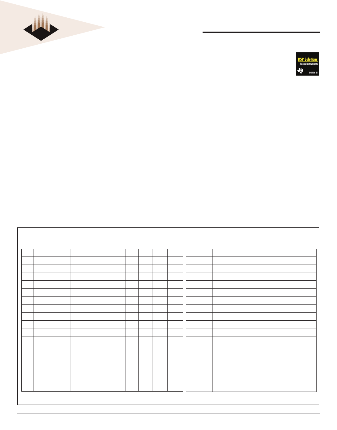
FIG. 1 PIN CONFIGURATION
TOP VIEW
1
2
3
4
5
67 8 9
A DQ19 DQ23 VCC VSS
VSS VSS VCC DQ24 DQ28
B DQ18 DQ22 VCC VSS SDCE# VSS VCC DQ25 DQ29
C VCCQ VCCQ VCC SDWE# SDA10 NC VCC VCCQ VCCQ
D DQ17 DQ21 VCC VSS
VSS VSS VCC DQ26 DQ30
E DQ16 DQ20 VCC VSS SDCK VSS VCC DQ27 DQ31
F VCCQ
VCCQ
VCC
VSS
VSS
VSS VCC VCCQ VCCQ
G NC
NC
NC SDRAS# SDCAS# VSS A2 A4 A5
H NC
NC
A8
VSS
VSS NC A1 A3 A10
J
A6
A7
A9
VSS
VSS NC A0 A11 A12
K A17 NC/A18 NC/A19 VSS
VSS NC NC A13 A14
L NC
NC
NC BWE2# BWE3# NC NC A15 A16
M VCCQ VCCQ VCC BWE0# BWE1# NC VCC VCCQ VCCQ
N DQ12 DQ11 VCC VSS
VSS VSS VCC DQ4 DQ0
P DQ13 DQ10 VCC VSS SSCK VSS VCC DQ5 DQ1
R VCCQ
VCCQ
VCC
VSS
VSS
VSS VCC VCCQ VCCQ
T DQ14 DQ9 VCC SSADC# SSWE# NC VCC DQ6 DQ2
U DQ15
DQ8
VCC SSOE# SSCE# NC VCC DQ7 DQ3
A0-17
DQ0-31
SSCK#
SSADC#
SSWE#
SSOE#
SDCK
SDRAS#
SDCAS#
SDWE#
SDA10
BWE0-3#
SSCE
SDCE
VCC
VCCQ
VSS
NC
PIN DESCRIPTION
Address Bus
Data Bus
SSRAM Clock
SSRAM Address Status Control
SSRAM Write Enable
SSRAM Output Enable
SDRAM Clock
SDRAM Row Address Strobe
SDRAM Column Address Strobe
SDRAM Write Enable
SDRAM Address 10/auto precharge
SSRAM Byte Write Enables SDRAM SDQM 0-3
Chip Enable SSRAM Device
Chip Enable SDRAM Device
Power Supply pins, 3.3V
Data Bus Power Supply pins, 3.3V (2.5V future)
Ground
No Contact
Contact factory for ordering information.
White Electronic Designs Corp. reserves the right to change products or specifications without notice.
September, 2003
Rev. 1
1
White Electronic Designs Corporation • (602) 437-1520 • www.wedc.com
Share Link: 