WED9LC6816V1310BC 查看數據表(PDF) - White Electronic Designs => Micro Semi
零件编号
产品描述 (功能)
生产厂家
WED9LC6816V1310BC Datasheet PDF : 27 Pages
| |||
White Electronic Designs
WED9LC6816V
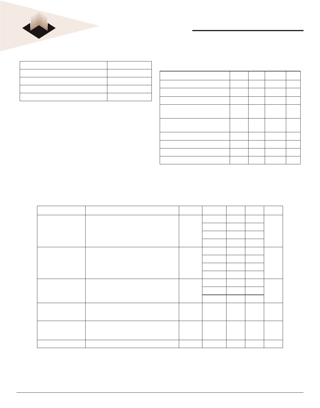
Absolute Maximum Ratings
Voltage on VCC Relative to VSS
-0.5V to +4.6V
VIN (DQx)
-0.5V to Vcc +0.5V
Storage Temperature (BGA)
-55°C to +125°C
Junction Temperature
+150°C
Short Circuit Output Current
100 mA
*Stress greater than those listed under "Absolute Maximum Ratings" may cause
permanent damage to the device. This is a stress rating only and functional
operation of the device at these or any other conditions greater than those indicated
in operational sections of this specifications is not implied. Exposure to absolute
maximum rating conditions for extended periods may affect reliability.
Recommended DC Operating Conditions
(Vcc = 3.3V -5% / +10% unless otherwise noted;
0°C Ta 70°C, Commercial; -40°C Ta 85°C, Industrial)
Parameter
Symbol Min Max Units
Supply Voltage (1)
VCC 3.135 3.6
V
Input High Voltage (1,2)
VIH
2.0 VCC +0.3 V
Input Low Voltage (1,2)
VIL
-0.3
0.8
V
Input Leakage Current
0 VIN VCC
ILI
-10
10
A
Output Leakage (Output Disabled)
ILO
-10
10
A
0 VIN VCC
SSRAM Output High (IOH = -4mA) (1) VOH 2.4
—
V
SSRAM Output Low (IOL = 8mA) (1) VOL
—
0.4
V
SDRAM Output High (IOH = -2mA)
VOH
2.4
—
V
SDRAM Output Low (IOL = 2mA)
VOL
—
0.4
V
NOTES:
1. All voltages referenced to VSS (GND).
2. Overshoot: VIH +6.0V for t tKC/2 Underershoot: VIL -2.0V for
t tKC/2
DC Electrical Characteristics
(Vcc = 3.3V -5% / +10% unless otherwise noted; 0°C Ta 70°C, Commercial; -40°C Ta 85°C, Industrial)
Description
Conditions
Symbol Frequency Typ Max Units
133MHz 500 625
Power Supply Current
Operating (1, 2, 3)
SSRAM Active / DRAM Auto Refresh
150MHz 500 650
ICC1
mA
166MHz 550 700
200MHz 600 800
133MHz 325 425
Power Supply Current
Operating (1, 2, 3)
SSRAM Active / DRAM Idle
150MHz 350 450
ICC2
mA
166MHz 400 495
200MHz 450 585
Power Supply Current
Operating (1, 2, 3)
SSRAM Active / SSRAM Idle
83MHz 500 625
ICC3
100MHz 500
650
mA
125MHz 550 700
CMOS Standby
SSCE# and SDCE# VCC -0.2V,
All other inputs at VSS +0.2 VIN or
ISB1
VIN VCC -0.2V, Clk frequency = 0
20.0 40.0 mA
TTL Standby
Auto Refresh
SSCE# and SDCE# VIH min
All other inputs at VIL max VIN or
ISB2
VIN VCC -0.2V, CK# frequency = 0
ICC5
30.0 55.0 mA
250
300
mA
NOTES:
1. ICC (operating) is specified with no output current. ICC (operating) increases with faster cycle times and greater output loading.
2. "Device idle" means device is deselected (CE# = VIH) Clock is running at max frequency and Addresses are switching each cycle.
3. Typical values are measured at 3.3V, 25°C. ICC (operating) is specified at specified frequency.
Contact factory for ordering information.
White Electronic Designs Corp. reserves the right to change products or specifications without notice.
September, 2003
Rev. 1
4
White Electronic Designs Corporation • (602) 437-1520 • www.wedc.com
Share Link: 