M48Z32VMT(2007) жҹҘзңӢж•ёж“ҡиЎЁпјҲPDFпјү - STMicroelectronics
йӣ¶д»¶зј–еҸ·
дә§е“ҒжҸҸиҝ° (еҠҹиғҪ)
з”ҹдә§еҺӮ家
M48Z32VMT Datasheet PDF : 19 Pages
| |||
Operating modes
M48Z32V
Table 4. Write mode AC characteristics
Symbol
Parameter(1)
M48Z32V
вҖ“35
Min
Max
tAVAV
tAVWL
tAVEL
tWLWH
tELEH
tWHAX
tEHAX
tDVWH
tDVEH
tWHDX
tEHDX
tWLQZ(2)(3)
tAVWH
tAVEH
tWHQX(2)(3)
WRITE cycle time
Address valid to WRITE enable low
Address valid to chip enable low
WRITE enable pulse width
Chip enable low to chip enable high
WRITE enable high to address transition
Chip enable high to address transition
Input valid to WRITE enable high
Input valid to chip enable high
WRITE enable high to input transition
Chip enable high to input transition
WRITE enable low to output Hi-Z
Address valid to WRITE enable high
Address valid to chip enable high
WRITE enable high to output transition
35
0
0
25
25
0
0
12
12
0
0
13
25
25
5
1. Valid for ambient operating temperature: TA = 0 to 70В°C; VCC = 3.0 to 3.6V (except where noted).
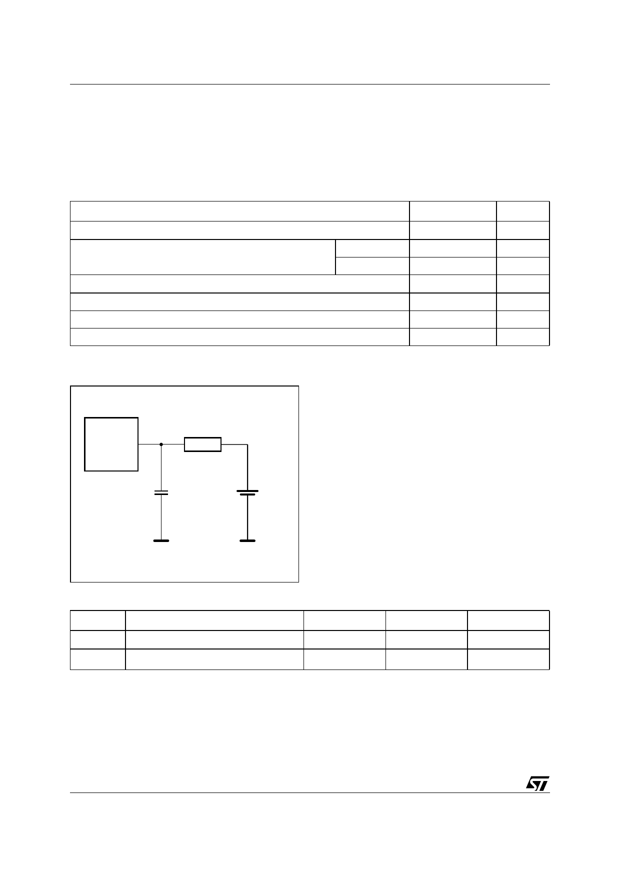
2. CL = 5pF (see Figure 8 on page 16).
3. If E goes low simultaneously with W going low, the outputs remain in the high impedance state.
Unit
ns
ns
ns
ns
ns
ns
ns
ns
ns
ns
ns
ns
ns
ns
ns
2.3
Note:
Data retention mode
With valid VCC applied, the M48Z32V operates as a conventional BYTEWIDEв„ў static RAM.
Should the supply voltage decay, the RAM will automatically power-fail deselect, write
protecting itself when VCC falls within the VPFD (max), VPFD (min) window. All outputs
become high impedance, and all inputs are treated as вҖңDon't care.вҖқ
A power failure during a WRITE cycle may corrupt data at the currently addressed location,
but does not jeopardize the rest of the RAM's content. At voltages below VPFD(min), the
user can be assured the memory will be in a write protected state, provided the VCC fall time
is not less than tF. The M48Z32V may respond to transient noise spikes on VCC that reach
into the deselect window during the time the device is sampling VCC. Therefore, decoupling
of the power supply lines is recommended.
When VCC drops below VSO, the control circuit switches power to the external battery which
preserves data.
As system power returns and VCC rises above VSO, the battery is disconnected, and the
power supply is switched to external VCC. Write protection continues until VCC reaches
VPFD(min) plus tREC(min). Normal RAM operation can resume tREC after VCC exceeds
VPFD(max).
For more information on Battery Storage Life refer to the Application Note AN1012.
10/19
Share Link: 