LCX037BLT 查看數據表(PDF) - Sony Semiconductor
零件编号
产品描述 (功能)
生产厂家
LCX037BLT Datasheet PDF : 25 Pages
| |||
LCX037BLT
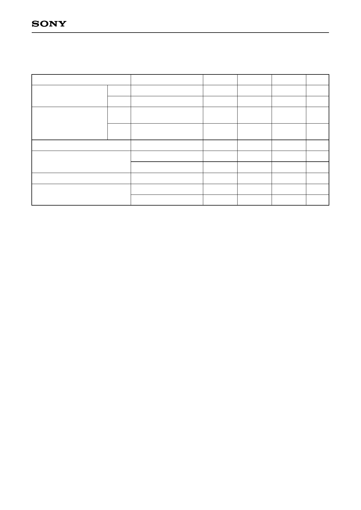
Input Signals
1. Input signal voltage conditions (VSS = 0V)
Item
Symbol
H shift register input voltage (Low) VHIL
HST, HCK1, HCK2, RGT (High) VHIH
Min.
Typ.
Max.
Unit
–0.5
0.0
0.4
V
4.5
5.0
5.5
V
V shift register input voltage (Low)
VB1, VB2, BLK, VST,
VCK, PCG, ENB, DWN (High)
VVIL
VVIH
–0.5
0.0
4.5
5.0
0.4
V
5.5
V
Video signal center voltage
Video signal input range∗1
Common voltage of panel∗2
Uniformity improvement signal
input voltage∗3
VVC
Vsig1, 3, 5, 7, 9, 11
Vsig2, 4, 6, 8
Vcom
Vpsig1, 3
Vpsig2, 4
7.4
7.5
7.6
V
VVC ± 4.4 VVC ± 4.5 VVC ± 4.6 V
VVC ± 4.4 VVC ± 4.5 VVC ± 4.6 V
VVC – 0.8 VVC – 0.7 VVC – 0.6 V
VVC ± 4.4 VVC ± 4.5 VVC ± 4.6 V
VVC ± 2.3 VVC ± 2.5 VVC ± 2.7 V
∗1 Input video signal shall be symmetrical to VVC.
∗2 The typical value of the common pad voltage may lower its suitable voltage according to the set
construction to use. In this case, use the voltage of which has maximum contrast as typical value.
When the typical value is lowered, the maximum and minimum values may lower.
–6–
Share Link: 