CA3160 查看數據表(PDF) - Intersil
零件编号
产品描述 (功能)
生产厂家
CA3160 Datasheet PDF : 17 Pages
| |||
CA3160, CA3160A
Absolute Maximum Ratings
Thermal Information
Supply Voltage (Between V+ and V- Terminals) . . . . . . . . . . . +16V
Differential Mode Input Voltage . . . . . . . . . . . . . . . . . . . . . . . . . . .8V
Input Voltage . . . . . . . . . . . . . . . . . . . . . . . . . (V+ +8V) to (V- -0.5V)
Input Current . . . . . . . . . . . . . . . . . . . . . . . . . . . . . . . . . . . . . . . 1mA
Output Short Circuit Duration (Note 2). . . . . . . . . . . . . . . . Indefinite
Operating Conditions
Temperature Range . . . . . . . . . . . . . . . . . . . . . . . . . -55oC to 125oC
Thermal Resistance (Typical, Note 1)
θJA (oC/W) θJC (oC/W)
PDIP Package . . . . . . . . . . . . . . . . . . . 110
N/A
Metal Can Package . . . . . . . . . . . . . . . 170
85
Maximum Junction Temperature (Metal Can). . . . . . . . . . . . . . .175oC
Maximum Junction Temperature (Plastic Package) . . . . . . . .150oC
Maximum Storage Temperature Range . . . . . . . . . . -65oC to 150oC
Maximum Lead Temperature (Soldering 10s) . . . . . . . . . . . . 300oC
CAUTION: Stresses above those listed in “Absolute Maximum Ratings” may cause permanent damage to the device. This is a stress only rating and operation of the
device at these or any other conditions above those indicated in the operational sections of this specification is not implied.
NOTES:
1. θJA is measured with the component mounted on an evaluation PC board in free air.
2. Short Circuit may be applied to ground or to either supply.
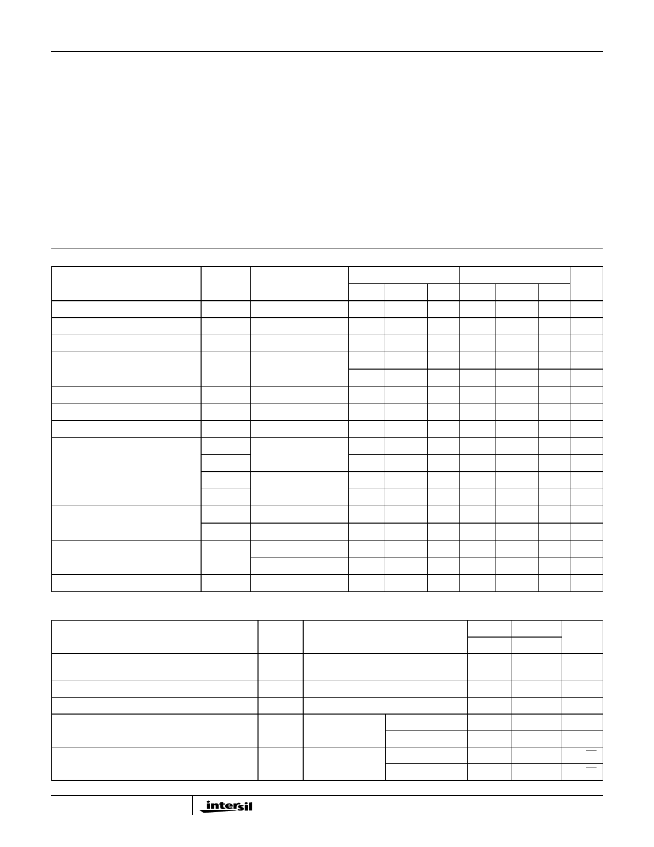
Electrical Specifications TA = 25oC, V+ = 15V, V- = 0V, Unless Otherwise Specified
CA3160
CA3160A
PARAMETER
SYMBOL TEST CONDITIONS MIN
TYP MAX MIN
TYP MAX UNITS
Input Offset Voltage
Input Offset Current
Input Current
Large-Signal Voltage Gain
|VIO| VS = ±7.5V
-
|IIO|
VS = ±7.5V
-
II
VS = ±7.5V
-
AOL VO = 10VP-P, RL = 2kΩ
50
94
6
15
-
0.5
30
-
5
50
-
320
-
50
110
-
94
2
5
mV
0.5
20
pA
5
30
pA
320
- kV/V
110
-
dB
Common-Mode Rejection Ratio
CMRR
70
90
-
80
95
-
dB
Common-Mode Input-Voltage Range
Power-Supply Rejection Ratio
Maximum Output Voltage
Maximum Output Current
Supply Current (Note 3)
Input Offset Voltage Temperature Drift
VlCR
PSRR
VOM+
VOM-
VOM+
VOM-
IOM+
IOM-
I+
∆VIO/∆VS, VS = ±7.5V
RL = 2kΩ
RL = ∞
VO = 0V (Source)
VO = 15V (Sink)
VO = 7.5V, R L = ∞
VO = 0V, R L = ∞
∆VIO/∆T
0 -0.5 to 12 10
-
32
320
12
13.3
-
-
0.002 0.01
14.99
15
-
-
0
0.01
12
22
45
12
20
45
-
10
15
-
2
3
-
8
-
0 -0.5 to 12 10
V
-
32
150 µV/V
12
13.3
-
V
-
0.002 0.01 V
14.99
15
-
V
-
0
0.01 V
12
22
45 mA
12
20
45 mA
-
10
15 mA
-
2
3
mA
-
6
- µV/oC
Electrical Specifications For Design Guidance, VSUPPLY = ±7.5V, TA = 25oC, Unless Otherwise Specified
CA3160
PARAMETER
SYMBOL
TEST CONDITIONS
TYP
Input Offset Voltage Adjustment Range
10kΩ Across Terminals 4 and 5 or
±22
Terminals 4 and 1
Input Resistance
Input Capacitance
Equivalent Input Noise Voltage
Equivalent Input Noise Voltage
RI
1.5
CI
f = 1MHz
4.3
eN BW = 0.2MHz
RS = 1MΩ
40
RS = 10MΩ
50
eN RS = 100Ω
1kHz
72
10kHz
30
CA3160A
TYP
±22
1.5
4.3
40
50
72
30
UNITS
mV
TΩ
pF
µV
µV
nV/√Hz
nV/√Hz
2
Share Link: 