CA3272A 查看數據表(PDF) - Intersil
零件编号
产品描述 (功能)
生产厂家
CA3272A Datasheet PDF : 10 Pages
| |||
CA3272A, CA3292A
RLOAD(max) = [VSUPPLY(min) - VTHD(max)] / ICEX(max) (EQ. 3)
RLOAD(max) = (6.5V - 5.5V) / 100µA = 10kΩ
(EQ. 4)
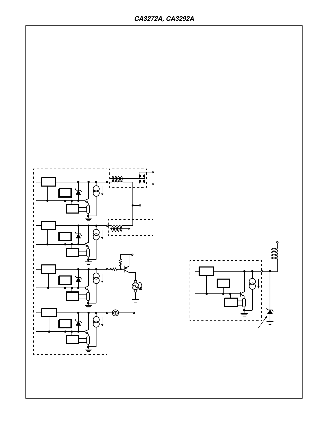
Since the CA3272A do not have on-chip diodes to clamp
voltage spikes which may be generated during inductive
switching of the load circuit, an external Zener diode (30V or
less is recommended) should be connected between the
output terminal and ground. Only those outputs used to
switch inductive loads require this protection. Note that since
the rate of change of output current is very high, even small
values of inductance can generate voltage spikes of consid-
erable amplitude on the output terminals which may require
clamping. External free-wheeling diodes returned to the sup-
ply voltage are generally not acceptable as inductive clamps
if the supply voltage exceeds 30V during transients. Typical
loads for either the CA3272A or CA3292A are shown in the
application circuit of Figure 4A. Where inductive loads are
driven from outputs A and B, no external Zener diode clamp
is needed for the CA3292A but is required for the CA3272A
as shown in Figure 4B.
The CA3272A and CA3292A are supplied in specially con-
figured power packages to conduct heat from the junction
through the mounting structure and device leads to the PC
Board. The ground leads are directly connected to the
mounting pad of the chip. The junction-to-air thermal resis-
tance, θJA may be significantly improved by suitable layout
design of the PC board to which the package is soldered.
Two or more square inches of PC Board ground area next to
the device ground pins is recommended. The PC Board
ground layer should be on the device side of the board with
open space for heat radiation.
Refer to Application Note AN9416 for additional thermal
information. Further information is provided on pulse energy
calculation methods for inductive load applications with
detail explaining the Safe Operating Area shown in Figure 5.
The SOA area for single energy transients is below the dot-
ted lines for the given ambient temperature conditions. The
energy locus plots of the three inductive coils were made for
arbitrarily chosen values of inductance and are shown here
for reference information. The RL time constant, ambient
temperature, clamp voltage and the stored energy in the coil
determine the SOA limits.
FAULT
OUT A
ZA
TLIM
QA
ILIM
RELAY
+VBATT
FAULT
OUT B
ZB
TLIM
QB
ILIM
FAULT
OUT C
ZC
TLIM
QC
ILIM
SOLENOID
+VBATT
HIGH CURRENT
HIGH SIDE DR
MOTOR
FAULT
OUT D
ZD
TLIM
QD
ILIM
LAMP
CA3292A
+VBATT
+VBATT
INDUCTIVE
LOAD
FAULT
TLIM
ILIM
CA3272A
(1 OF 4 CHANNELS)
OUT A
QA
VZ(EXT)
EXTERNAL ZENER DIODE CLAMP
PROTECTION FROM POSITIVE VOLTAGE
SPIKE (INDUCTIVE KICK PULSE) AT TURN-OFF
NOTE: The internal drive circuit with self protection and fault output
is the CA3292A with the over voltage Zener diode clamp.
FIGURE 4A. TYPICAL APPLICATION CIRCUIT SHOWING OUT-
PUT LOAD CONTROL CAPABILITY OF THE
CA3272A OR CA3292A
NOTE: The VCE(SUS) voltage rating is the maximum voltage for full
load switching.
FIGURE 4B. CA3272A OVER-VOLTAGE PROTECTION IS AN
EXTERNAL ZENER DIODE CLAMP WHERE
VZ(EXT) ≤ VCE(SUS)
7
Share Link: 