CA3420E 查看數據表(PDF) - Intersil
零件编号
产品描述 (功能)
生产厂家
CA3420E Datasheet PDF : 6 Pages
| |||
CA3420, CA3420A
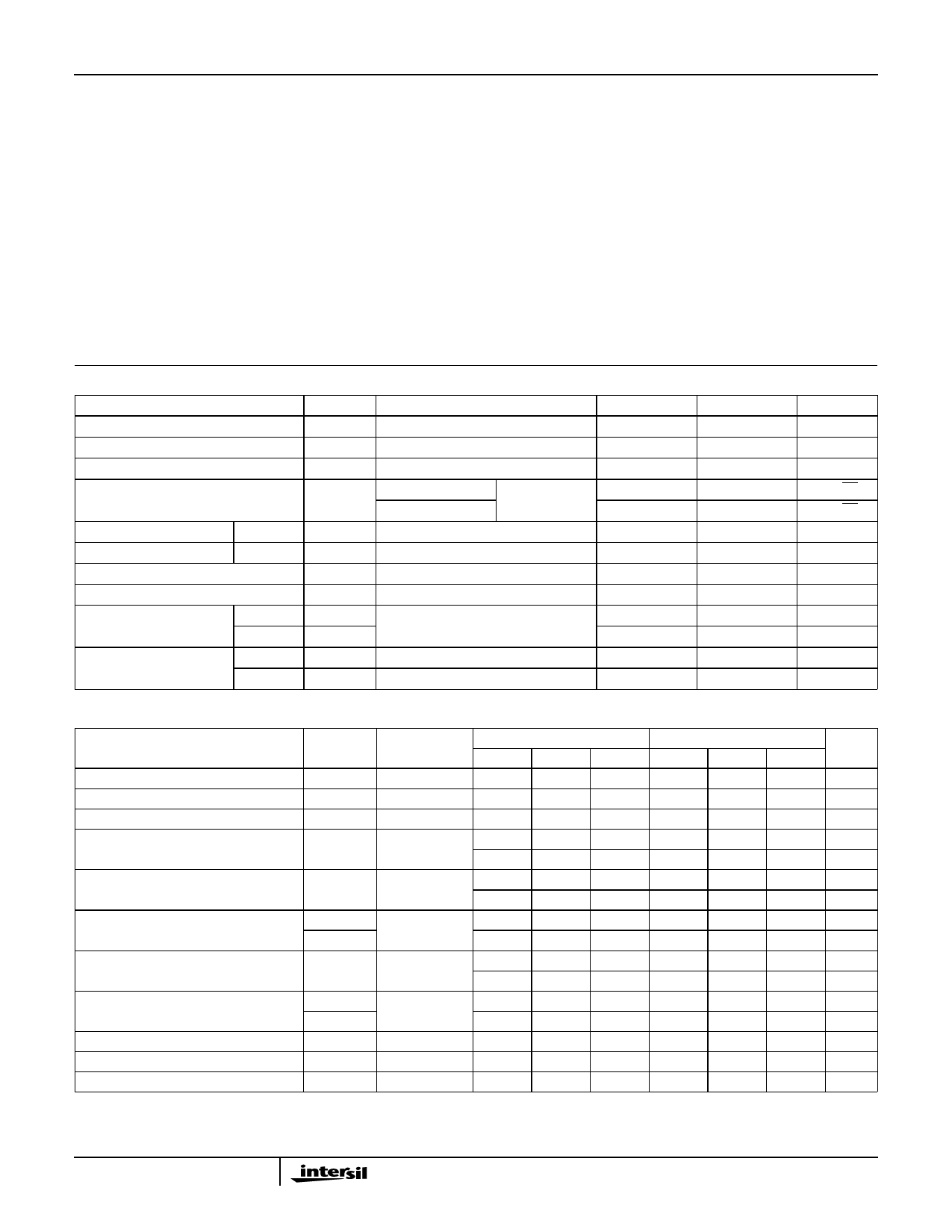
Absolute Maximum Ratings
Supply Voltage (V+ to V-). . . . . . . . . . . . . . . . . . . . . . . . . . . . . . .22V
Differential Input Voltage . . . . . . . . . . . . . . . . . . . . . . . . . . . . . . .15V
DC Input Voltage . . . . . . . . . . . . . . . . . . . . . . (V+ + 8V) to (V- -0.5V)
Input Current . . . . . . . . . . . . . . . . . . . . . . . . . . . . . . . . . . . . . . . 1mA
Output Short Circuit Duration (Note 1). . . . . . . . . . . . . . . . Indefinite
Operating Conditions
Temperature Range . . . . . . . . . . . . . . . . . . . . . . . . . -55oC to 125oC
Thermal Information
Thermal Resistance (Typical, Note 2)
θJA (oC/W) θJC (oC/W)
PDIP Package . . . . . . . . . . . . . . . . . . . 105
N/A
Metal Can Package . . . . . . . . . . . . . . . 165
80
Maximum Junction Temperature (Metal Can Package). . . . . . . 175oC
Maximum Junction Temperature (Plastic Package) . . . . . . . 150oC
Maximum Storage Temperature Range . . . . . . . . . . -65oC to 150oC
Maximum Lead Temperature (Soldering 10s) . . . . . . . . . . . . 300oC
CAUTION: Stresses above those listed in “Absolute Maximum Ratings” may cause permanent damage to the device. This is a stress only rating and operation of the
device at these or any other conditions above those indicated in the operational sections of this specification is not implied.
NOTES:
1. Short circuit may be applied to ground or to either supply.
2. θJA is measured with the component mounted on an evaluation PC board in free air.
Electrical Specifications Typical Values Intended Only for Design Guidance, VSUPPLY = ±10V, TA = 25oC
PARAMETER
SYMBOL
TEST CONDITIONS
CA3420A
CA3420
Input Resistance
RI
150
150
Input Capacitance
CI
4.9
4.9
Output Resistance
RO
300
300
Equivalent Input Noise Voltage
eN
f = 1kHz
RS = 100Ω
62
62
f = 10kHz
38
38
Short-Circuit Current
To Opposite Supply
Gain Bandwidth Product
Slew Rate
Source
Sink
IOM+
IOM-
fT
SR
2.6
2.6
2.4
2.4
0.5
0.5
0.5
0.5
Transient Response
Rise Time
Overshoot
tR
RL = 2kΩ, CL = 100pF
OS
0.7
0.7
15
15
Current from Terminal 8 To V-
I8+
To V+
I8-
20
20
2
2
UNITS
TΩ
pF
Ω
nV/√Hz
nV/√Hz
mA
mA
MHz
V/µs
µs
%
µA
mA
Electrical Specifications For Equipment Design, At VSUPPLY = ±1V, TA = 25oC, Unless Otherwise Specified
PARAMETER
TEST
SYMBOL CONDITIONS
CA3420
MIN
TYP
MAX
CA3420A
MIN
TYP
MAX
UNITS
Input Offset Voltage
Input Offset Current (Note 3)
Input Current (Note 3)
Large Signal Voltage Gain
|VIO|
|IIO|
|II|
AOL
RL = 10kΩ
-
5
10
-
0.01
4
-
1
5
10
100
-
80
100
-
-
2
-
0.01
-
0.02
20
100
86
100
5
mV
4
pA
5
pA
-
kV/V
-
dB
Common Mode Rejection Ratio
CMRR
-
560
1800
-
560
1000 µV/V
55
65
-
60
65
-
dB
Common Mode Input Voltage Range
Power Supply Rejection Ratio
Max Output Voltage
Supply Current
VlCR+
VlCR-
PSRR
∆VIO/∆V
VOM+
VOM-
I+
RL = ∞
0.2
-
-
60
0.90
-0.85
-
0.5
-1.3
100
80
0.95
-0.91
350
-
-
1000
-
-
-
650
0.2
-1
-
70
0.90
-0.85
-
0.5
-1.3
32
90
0.95
-0.91
350
-
V
-
V
320
µV/V
-
dB
-
V
-
V
650
µA
Device Dissipation
Input Offset Voltage Temperature Drift
NOTE:
PD
∆VlO/∆T
-
0.7
1.1
-
0.7
1.1
mW
-
4
-
-
4
-
µV/oC
3. The maximum limit represents the levels obtainable on high speed automatic test equipment. Typical values are obtained under laboratory conditions.
2
Share Link: 