CA3450 查看數據表(PDF) - Intersil
零件编号
产品描述 (功能)
生产厂家
CA3450 Datasheet PDF : 8 Pages
| |||
CA3450
Absolute Maximum Ratings
Thermal Information
Supply Voltage (Between V+ and V- Terminals) . . . . . . . . . . . 14.5V
Differential Input Voltage . . . . . . . . . . . . . . . . . . . . . . . . . . . . . . . .5V
Output Current . . . . . . . . . . . . . . . . . . . . . . . . . . . . . . . . . . . . 100mA
Operating Conditions
Temperature Range . . . . . . . . . . . . . . . . . . . . . . . . . . -40oC to 85oC
Thermal Resistance (Typical, Note 1)
θJA (oC/W)
PDIP Package . . . . . . . . . . . . . . . . . . . . . . . . . . . . .
60
Maximum Junction Temperature (Plastic Package) . . . . . . . .150oC
Maximum Storage Temperature Range . . . . . . . . . . -65oC to 150oC
Maximum Lead Temperature (Soldering 10s) . . . . . . . . . . . . 300oC
CAUTION: Stresses above those listed in “Absolute Maximum Ratings” may cause permanent damage to the device. This is a stress only rating and operation of the
device at these or any other conditions above those indicated in the operational sections of this specification is not implied.
NOTE:
1. θJA is measured with the component mounted on an evaluation PC board in free air.
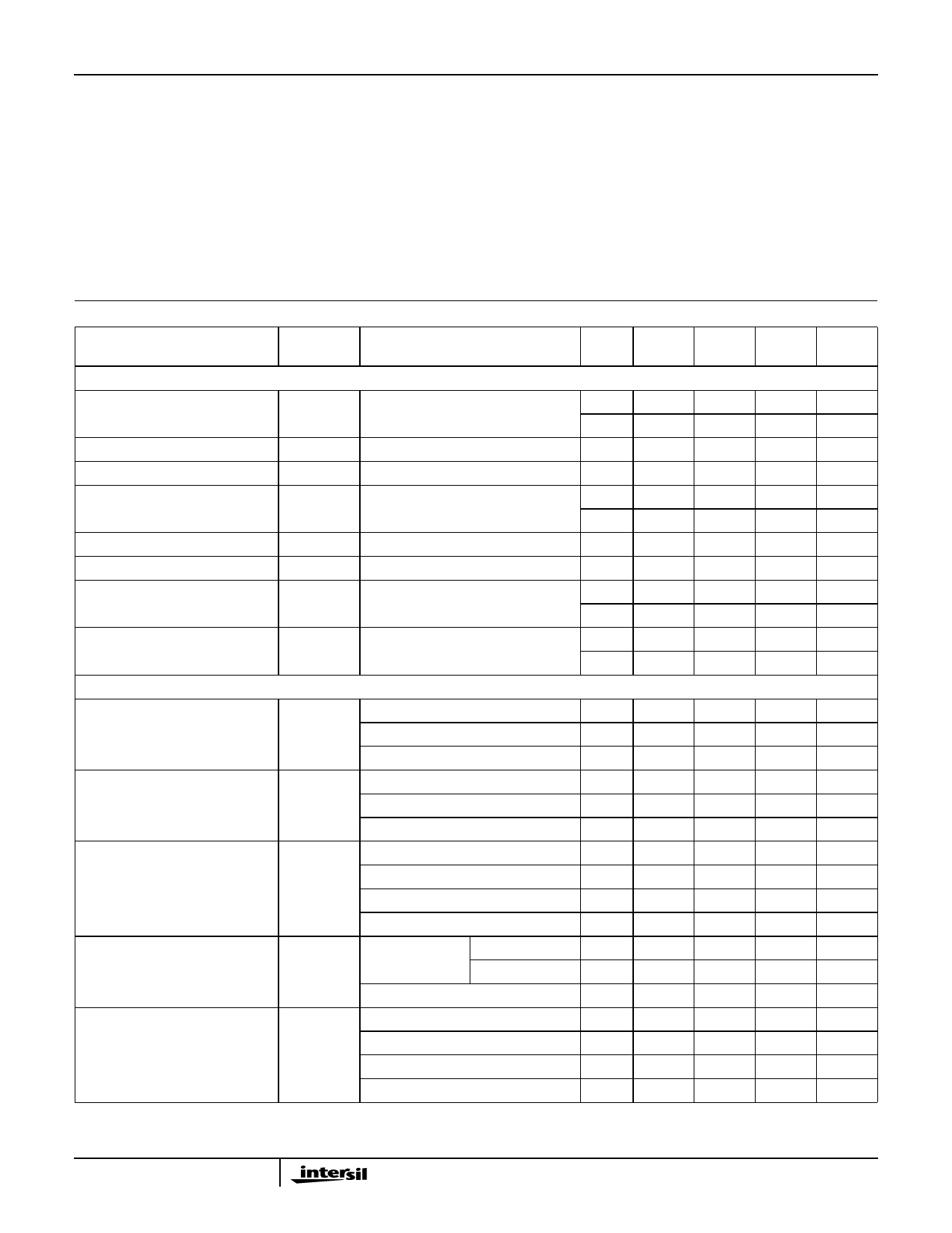
Electrical Specifications CC = 5pF, VSUPPLY = ±6V, Unless Otherwise Specified
PARAMETER
SYMBOL
TEST CONDITIONS
TEMP.
(oC)
MIN
TYP
MAX UNITS
DC
Input Offset Voltage
|VIO|
25
-
Full
-
8
20
mV
10
35
mV
Input Bias current
Input Offset Current
Open Loop DC Gain
|IIB|
|IIO|
AOL
VOUT = ±2.5V, RL = 50Ω
25
-
100
400
nA
25
-
50
200
nA
25
60
70
-
dB
Full
55
-
-
dB
Power Supply Rejection Ratio
PSRR ∆V = ±1V
25
55
65
-
dB
Common Mode Rejection Ratio
Common Mode Input Range
CMRR
VICR
VICR = ±3.5V
25
50
60
-
dB
25
±3.5
±3.7
-
V
Full
±3.0
-
-
V
Supply Current
I+
25
-
30
40
mA
Full
-
-
50
mA
DYNAMIC
-3dB Bandwidth
AV = 1 (See Figure 2)
CC = 5pF
Bandwidth (Unity Gain Crossing)
AV = Open Loop
CC = 0 (See Figure 1)
Bandwidth (Unity Gain Crossing)
AV = 10, CC = 0pF
RFEEDBACK = 450Ω
RPIN 3 - G = 50Ω (See Figure 2)
No Load
RL = 1MΩ||20pF
RL = 50Ω||20pF
No Load
RL = 20pF||1MΩ
RL = 50Ω||20pF
No Load
50Ω
1M||20pF
50Ω||1M||20pF
25
-
200
-
MHz
25
-
190
-
MHz
25
-
185
-
MHz
25
210
230
-
MHz
25
180
200
-
MHz
25
180
220
-
MHz
25
200
210
-
MHz
25
175
190
-
MHz
25
180
195
-
MHz
25
170
188
-
MHz
Transient Response, Overshoot
OS
AV = 1, CC = 5pF RL = 50Ω||20pF
25
-
30
-
%
(See Figure 3)
No Load
25
-
20
-
%
Settling Time (See Figure 5)
(2V Step, RL = 50Ω||20pF)
AV ≥10, CC = 0pF, RL = 50Ω||20pF
25
-
10
-
%
tS
AV = -1, CC = 5pF, 0.1%, 10 Bits
25
-
35
-
ns
AV = 1, CC = 5pF, 0.1%, 10 Bits
25
-
50
-
ns
AV = 10, CC = 0pF, 0.1%, 10 Bits
25
-
35
-
ns
AV = 10, CC = 0pF, 1.0%, 7 Bits
25
-
25
-
ns
3
Share Link: 