CA5130A 查看數據表(PDF) - Intersil
零件编号
产品描述 (功能)
生产厂家
CA5130A Datasheet PDF : 19 Pages
| |||
CA5130, CA5130A
+15V
10kΩ
3
+
7
0.01µF
6
2
-
8
56pF
4
5
1
100kΩ
OFFSET
ADJUST
2kΩ
0.1µF
0V
0V
0V
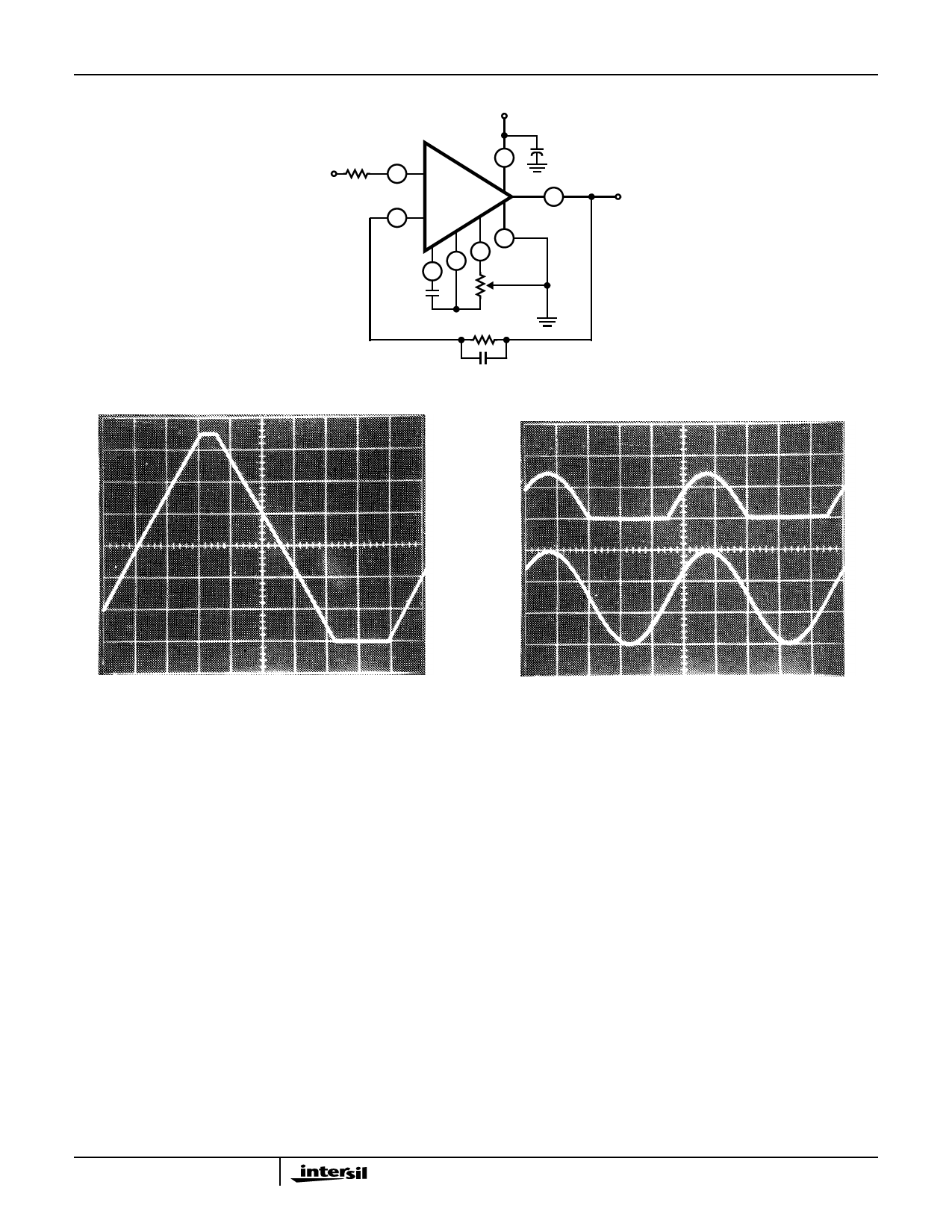
2V/Div., 500µs/Div.
Top Trace: Output = 5V/Div., 200µs/Div.
Bottom Trace: Input = 5V/Div., 200µs/Div.
FIGURE 4A. OUTPUT WAVEFORM WITH INPUT SIGNAL
RAMPING
FIGURE 4B. OUTPUT WAVEFORM WITH GROUND REFERENCE
SINE WAVE INPUT
FIGURE 4. SINGLE SUPPLY VOLTAGE FOLLOWER WITH ASSOCIATED WAVEFORMS. (e.g., FOR USE IN SINGLE SUPPLY
D/A CONVERTER; SEE FIGURE 9 IN AN6080)
The circuit uses an R/2R voltage ladder network, with the
output potential obtained directly by terminating the ladder
arms at either the positive or the negative power supply
terminal. Each CD4007A contains three “inverters”, each
“inverter” functioning as a single pole double throw switch to
terminate an arm of the R/2R network at either the positive or
negative power supply terminal. The resistor ladder is an
assembly of one percent tolerance metal oxide film resistors.
The five arms requiring the highest accuracy are assembled
with series and parallel combinations of 806,000Ω resistors
from the same manufacturing lot.
A single 15V supply provides a positive bus for the CA5130
follower amplifier and feeds the CA3085 voltage regulator. A
“scale adjust” function is provided by the regulator output
control, set to a nominal 10V level in this system. The line
voltage regulation (approximately 0.2%) permits a 9-bit
accuracy to be maintained with variations of several volts in
the supply. The flexibility afforded by the CMOS building
blocks simplifies the design of DAC systems tailored to
particular needs.
Single Supply, Absolute Value, Ideal Full Wave
Rectifier
The absolute value circuit using the CA5130 is shown in Figure
6. During positive excursions, the input signal is fed through the
feedback network directly to the output. Simultaneously, the
positive excursion of the input signal also drives the output
terminal (No. 6) of the inverting amplifier in a negative going
excursion such that the 1N914 diode effectively disconnects the
amplifier from the signal path. During a negative going
excursion of the input signal, the CA5130 functions as a normal
inverting amplifier with a gain equal to -R2/R1. When the
equality of the two equations shown in Figure 6 is satisfied, the
full wave output is symmetrical.
10
Share Link: 