CGY2014 查看數據表(PDF) - Philips Electronics
零件编号
产品描述 (功能)
生产厂家
CGY2014 Datasheet PDF : 12 Pages
| |||
Philips Semiconductors
GSM/DCS/PCS power amplifier
Preliminary specification
CGY2014ATW
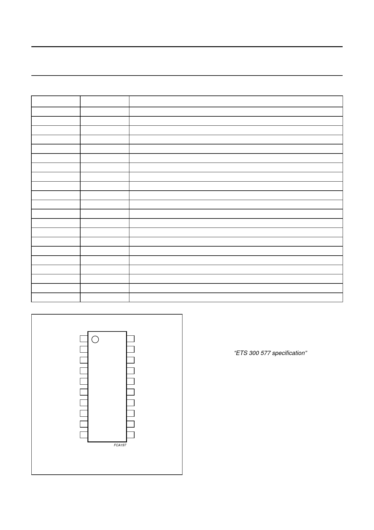
PINNING
SYMBOL
n.c.
RFI(HB)
VDD1(HB)
VDD2(HB)
VDD2(HB)
VDD2(LB)
VDD1(LB)
GND1(LB)
RFI(LB)
n.c.
VGLB
n.c.
RFO/VDD3(LB)
RFO/VDD3(LB)
GND
n.c.
RFO/VDD3(HB)
RFO/VDD3(HB)
n.c.
VGHB
−
PIN
1
2
3
4
5
6
7
8
9
10
11
12
13
14
15
16
17
18
19
20
exposed die
DESCRIPTION
not connected
DCS/PCS power amplifier input
DCS/PCS first stage supply voltage
DCS/PCS second stage supply voltage
DCS/PCS second stage supply voltage
GSM second stage supply voltage
GSM first stage supply voltage
GSM first stage ground
GSM power amplifier input
not connected
GSM power amplifier gates
not connected
GSM power amplifier output and third stage supply voltage
GSM power amplifier output and third stage supply voltage
ground
internal connection to ground; pin should not be connected to the board
DCS/PCS power amplifier output and third stage supply voltage
DCS/PCS power amplifier output and third stage supply voltage
not connected
DCS/PCS power amplifier gates
ground
handbook, halfpage
n.c. 1
RFI(HB) 2
20 VGHB
19 n.c.
VDD1(HB) 3
18 RFO/VDD3(HB)
VDD2(HB) 4
17 RFO/VDD3(HB)
VDD2(HB) 5
16 n.c.
CGY2014ATW
VDD2(LB) 6
15 GND
VDD1(LB) 7
14 RFO/VDD3(LB)
GND1(LB) 8
13 RFO/VDD3(LB)
RFI(LB) 9
12 n.c.
n.c. 10
11 VGLB
FCA197
Fig.2 Pin configuration.
FUNCTIONAL DESCRIPTION
Operating conditions
The CGY2014ATW is designed to meet the European
Telecommunications Standards Institute (ETSI) GSM
documents, the “ETS 300 577 specification”, which are
defined as follows:
• ton = 570 µs
• T = 4.16 ms
• Duty cycle δ = 1/8.
Multislot operation can be implemented provided that the
application circuit does not drive the IC beyond the limiting
values.
Power amplifier
The GSM and DCS/PCS power amplifiers consist of three
cascaded gain stages with an open-drain configuration.
Each drain has to be loaded externally by an adequate
reactive circuit which also has to be a DC path to the
supply.
2000 Nov 28
4
Share Link: 